Method for processing step ladder PCB plate

A PCB board and processing method technology, which is applied in the field of stepped PCB board processing, can solve the problems of unevenness, unstable glue flow in the ladder slot, and inability to remove the flow glue to block auxiliary materials, etc., so as to achieve easy removal and stable glue flow Effect

Active Publication Date: 2009-01-21
DONGGUAN SHENGYI ELECTRONICS
View PDF0 Cites 22 Cited by
  • Summary
  • Abstract
  • Description
  • Claims
  • Application Information

AI Technical Summary

Problems solved by technology

[0002] During the production process of stepped PCB boards, the adhesive flow in the stepped slots is unstable and uneven, which does not meet the design requirements of end customers and affects the placement of components
[0003] In order to solve the above technical problems, the existing technology uses auxiliary materials to block, but there is a problem that the flow glue flows to the bottom of the tank through the gap and the blocking auxiliary materials cannot be taken out.

Method used


Image

  • Method for processing step ladder PCB plate
  • Method for processing step ladder PCB plate

Examples


Embodiment Construction

[0017] The present invention will be described in detail below in conjunction with the accompanying drawings.

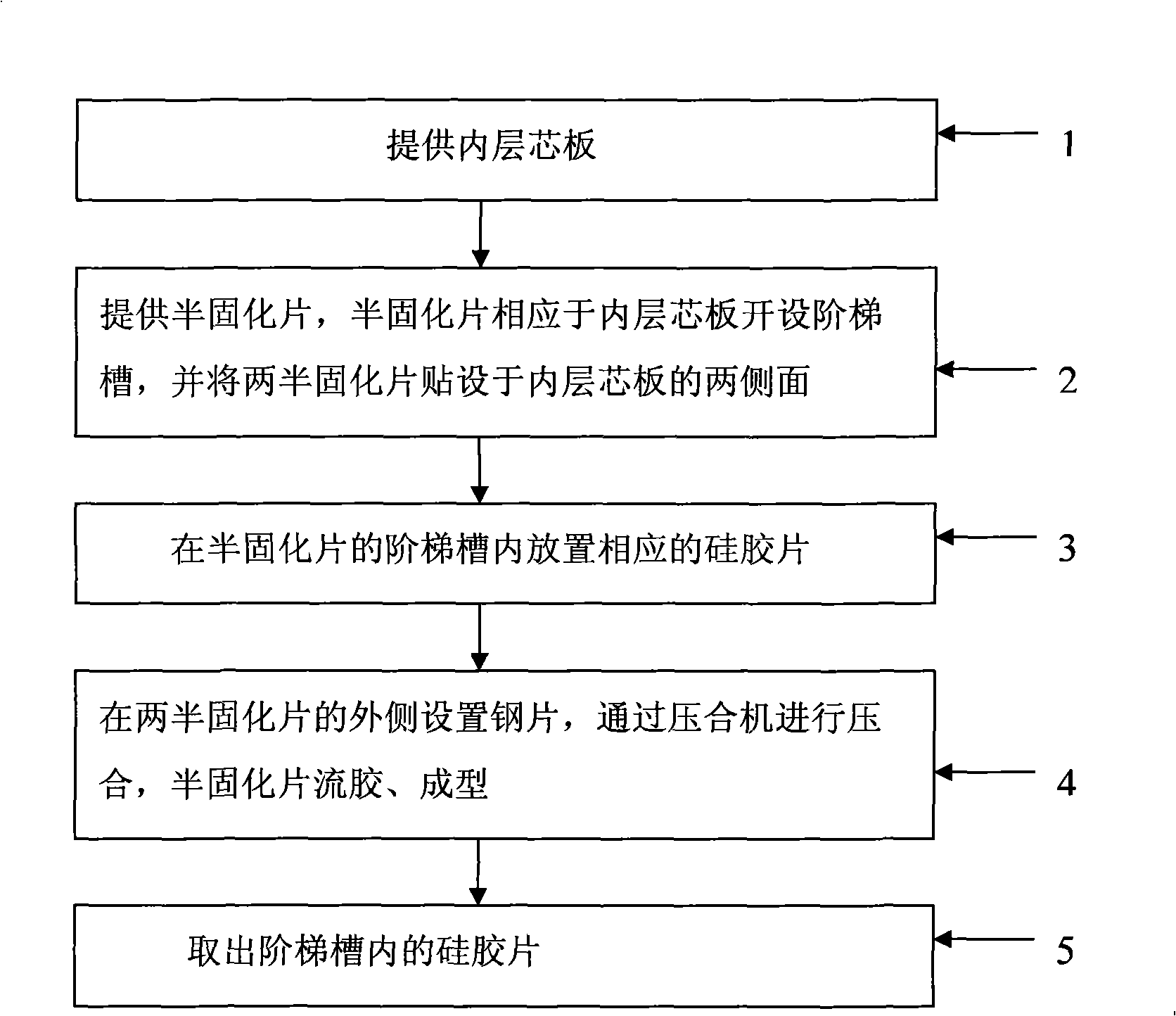
[0018] like Figure 1-2 Shown, the processing method of ladder PCB board of the present invention comprises the following steps:

[0019] Step 1: Provide inner core board; common inner core board can be used.

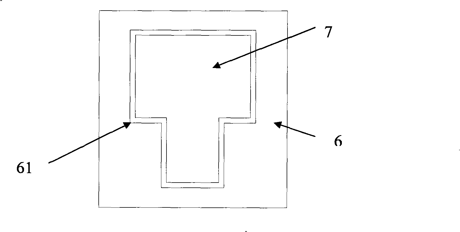
[0020] Step 2: Provide a prepreg. The prepreg is provided with stepped grooves corresponding to the inner core board, and the two prepregs are attached to both sides of the inner core board; refer to figure 2 , in this step, the prepreg 6 is provided with a stepped groove 61 according to the ladder PCB board drawing and suitable pre-compensation, the prepreg is a low fluidity prepreg, and a suitable prepreg is selected to ensure the glue flow at the position of the stepped groove.

[0021] Step 3: Place the corresponding silicone sheet in the stepped groove of the prepreg; refer to figure 2 , in this step, the silica gel sheet 7 is selected according to t...


PUM


Abstract

The invention relates to a method for processing a ladder PCB plate, which includes the following steps: an inner layer core plate is provided; prepregs are provided; a ladder groove is arranged at the prepregs correspondingly with the inner layer core plate and the two prepregs are attached to the two sides of the inner layer core plate; corresponding silicon rubber slices are placed in the ladder groove of the prepregs; steel sheets are positioned at the external sides of the two prepregs and are pressed by a pressing machine which carries out the gummosis and molding to the prepregs; the silicon rubber slices are taken out of the ladder groove. The method for processing the ladder PCB plate fills the silicon rubber slices in the ladder groove of the prepregs to barrier the gummosis and ensures that the gummosis amount is stable, controllable and meets the design requirement of customers; in addition, the silicon rubber slices can be easily taken out without sticking to the bottom of the groove, are simple and effective and are convenient and suitable for processing the ladder PCB plate.

Description

technical field [0001] The invention relates to the field of printed circuit board manufacture, in particular to a method for processing a stepped PCB board. Background technique [0002] During the production process of stepped PCB boards, the adhesive flow in the stepped slots is unstable and uneven, which does not meet the design requirements of end customers and affects the placement of components. [0003] In order to solve the above technical problems, the existing technology adopts auxiliary materials to stop, but there is a problem that the flow glue flows to the bottom of the tank through the gap and the blocking auxiliary materials cannot be taken out. Contents of the invention [0004] The purpose of the present invention is to provide a method for processing a stepped PCB board, which uses silica gel sheets to fill the stepped grooves to block the flow of glue, so as to ensure a stable and controllable flow of glue, and at the same time, it can be easily taken ...

Claims


Application Information

Patent Timeline
Patent Type & Authority Applications(China)
IPC IPC(8): H05K1/09B32B37/15B32B37/10B32B15/04
Inventor 杜红兵
Owner DONGGUAN SHENGYI ELECTRONICS
Why Eureka
Try Eureka