Secure yield-aware design flow with annotated design libraries

A design and design system technology, applied in the field of yield evaluation of integrated circuit design and manufacturing, which can solve problems such as failure to consider process and time characteristics, evaluation design, and inability to compare

Active Publication Date: 2009-02-25
TAIWAN SEMICON MFG CO LTD
View PDF0 Cites 3 Cited by
  • Summary
  • Abstract
  • Description
  • Claims
  • Application Information

AI Technical Summary

Problems solved by technology

During this period, the yield rate has also changed over time, which is likely to be an improvement, and the evaluation made in different periods is related to the same point in time and cannot be compared, so it is also of no value, because the existing platform does not have Considering the process and time-dependent characteristics, even if a designer wants to make a trade-off between multiple possible designs, for example, a high-efficiency design and a high-yield design, the user still has no way to accurately determine the early Evaluate the possible outcomes of the design during the design phase

Method used


Image

  • Secure yield-aware design flow with annotated design libraries
  • Secure yield-aware design flow with annotated design libraries
  • Secure yield-aware design flow with annotated design libraries

Examples


Embodiment Construction

[0016] How to create and use the presently preferred embodiment is discussed in detail below. It should be appreciated, however, that the present invention provides many applicable innovative concepts, which can be embodied in a wide variety of specific contexts. The specific embodiments discussed herein are merely illustrative of specific ways to make and use the invention, and are not intended to limit the scope of the invention.

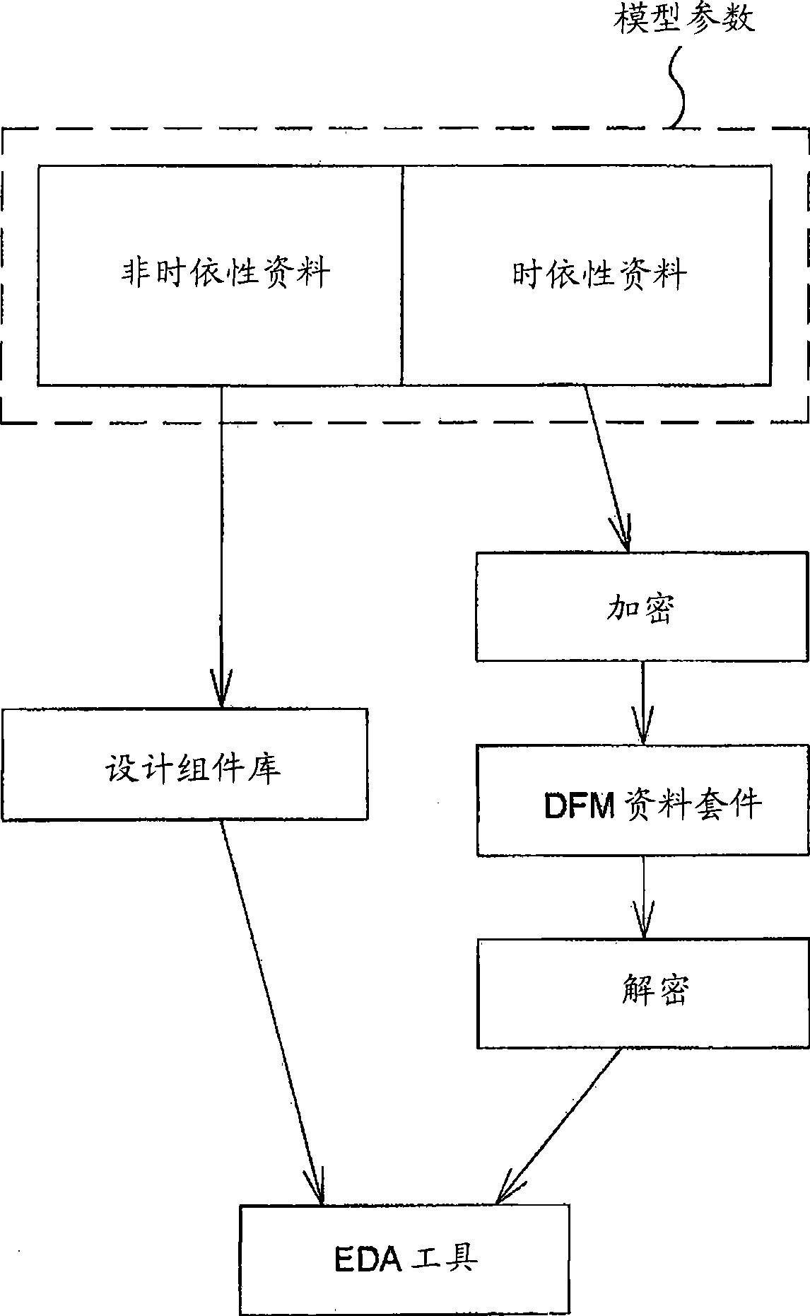
[0017] The interaction and communication between designers and manufacturers can achieve more accurate, faster, and more efficient designs by using Design for Manufacturability (or DFM). In one example, various manufacturing data will be formulated, quantified, and integrated to enhance collaboration between designers and manufacturers, reduce design time and cost, and improve manufacturing yield and production efficiency. DFM can be implemented in cooperation with design tool manufacturers at different design stages. The manufacturer can be a s...


PUM


Abstract

A method for designing and manufacturing integrated circuits is provided. The method includes providing a modeling parameter set for manufacturing an integrated circuit; dividing the modeling parameter set into time-dependent data and time-independent data; saving substantially all time-independent data into a design library; and saving substantially all time-dependent data into a design-for-manufacturing (DFM) data kit, wherein the DFM data kit is external to the design library.

Description

technical field [0001] The present invention relates to an integrated circuit manufacturing process, especially related to a design for manufacturability (design for manufacturing, DFM) system, and more particularly related to the yield evaluation of integrated circuit design and manufacturing. Background technique [0002] Design for Manufacturability is a development approach that emphasizes manufacturing issues in the product design process. Successful DFM results can reduce manufacturing costs from the early design stage without sacrificing product quality. [0003] Now there are more and more DFM aware designs. During the design phase, intermediate designs are typically taken offline to perform DFM checks to ensure that the design complies with the DFM, and to correct the design when problems are found. In the process of realizing full-chip fabrication, redesign scenarios also need to perform and repeat additional design sign-off analysis. For example, these steps wa...

Claims


Application Information

Patent Timeline
Patent Type & Authority Applications(China)
IPC IPC(8): G06F17/50
CPCG06F2217/12G06F17/5045G06F30/30G06F2119/18Y02P90/02
Inventor 傅宗民郑仪侃
Owner TAIWAN SEMICON MFG CO LTD
Why Eureka
Try Eureka