
Method for preventing memory array generating bit line interference

A memory array and bit line technology, applied in static memory, read-only memory, information storage, etc., can solve the problems of memory cell interference, increase of threshold voltage variation DVt, and influence on memory cell performance, so as to reduce potential difference, Improving the Effect of Bit Line Disturbance

Active Publication Date: 2009-02-25
SEMICON MFG INT (SHANGHAI) CORP
View PDF0 Cites 1 Cited by
  • Summary
  • Abstract
  • Description
  • Claims
  • Application Information

AI Technical Summary

Problems solved by technology

[0004] When a memory cell on a certain bit line needs to be programmed, it is easy to interfere with adjacent memory cells
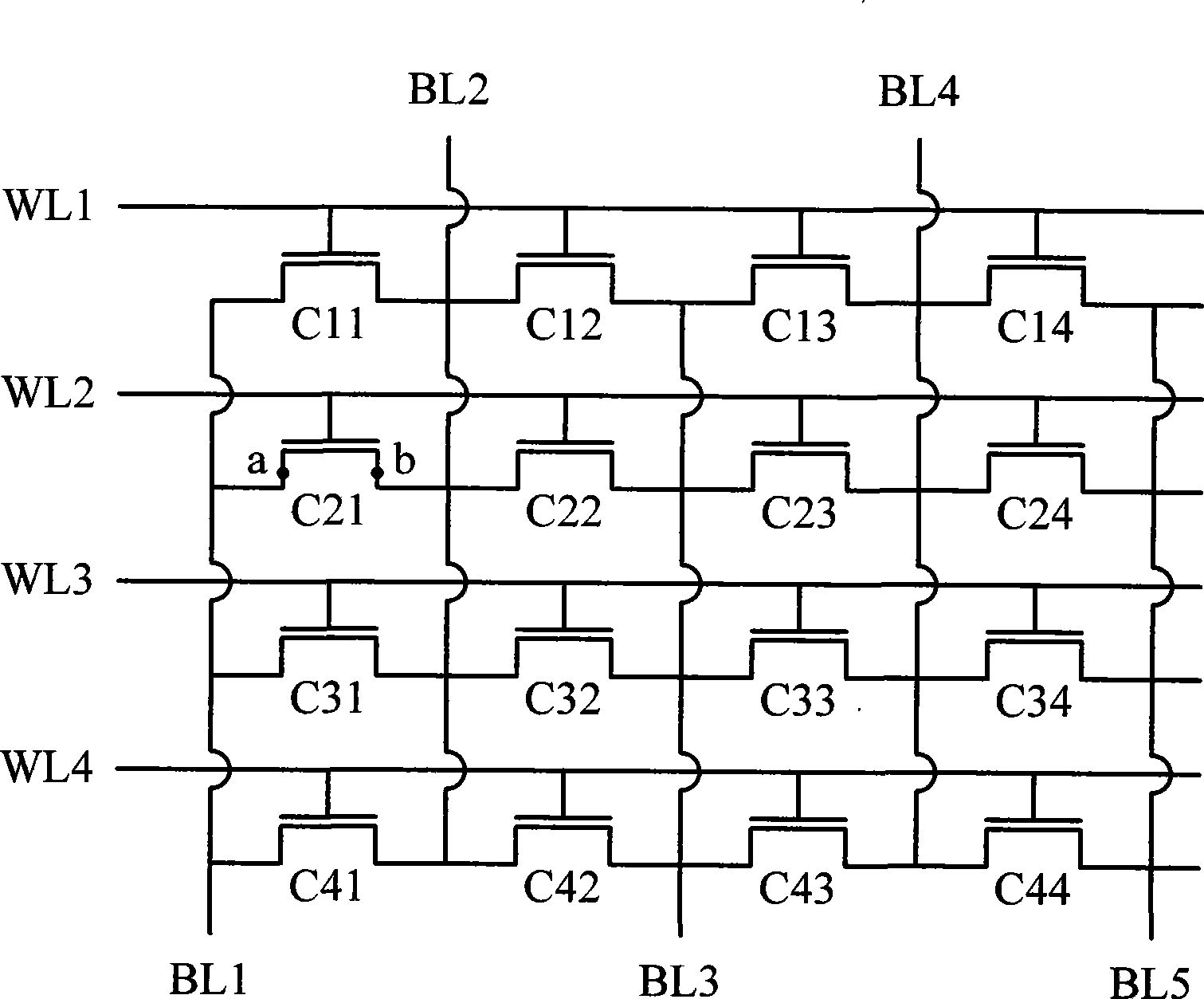
Taking the memory cell C11 as an example, a high potential needs to be applied to the bit line BL2 when programming it. Because the memory cells C21 and C11 share the bit lines BL1 and BL2, there will be a potential difference between the source and drain of C21. The potential difference will cause the threshold voltage variation DVt of the memory cell C21 to increase, thereby affecting the performance of the memory cell

Method used


Image

  • Method for preventing memory array generating bit line interference
  • Method for preventing memory array generating bit line interference
  • Method for preventing memory array generating bit line interference

Examples


Embodiment Construction

[0016] The method for preventing bit line interference in a memory array of the present invention will be further described in detail below.

[0017] The method of the present invention is that when a memory cell is receiving programming, if one of the two bit lines connected to its adjacent memory cell is at a high potential, and the other is at a floating state or a low potential, that is, there is a voltage between the source and the drain. When there is a potential difference, a gate bias voltage Vg is applied to the memory cell.

[0018] see figure 2 For example, when the memory cell C11 is being programmed, the bit line BL2 is at a high potential, the bit line BL1 is at a low potential, and the bit line BL3 is in a floating state. At this time, the memory cells C21 and C22 are disturbed. Apply gate bias voltage Vg.

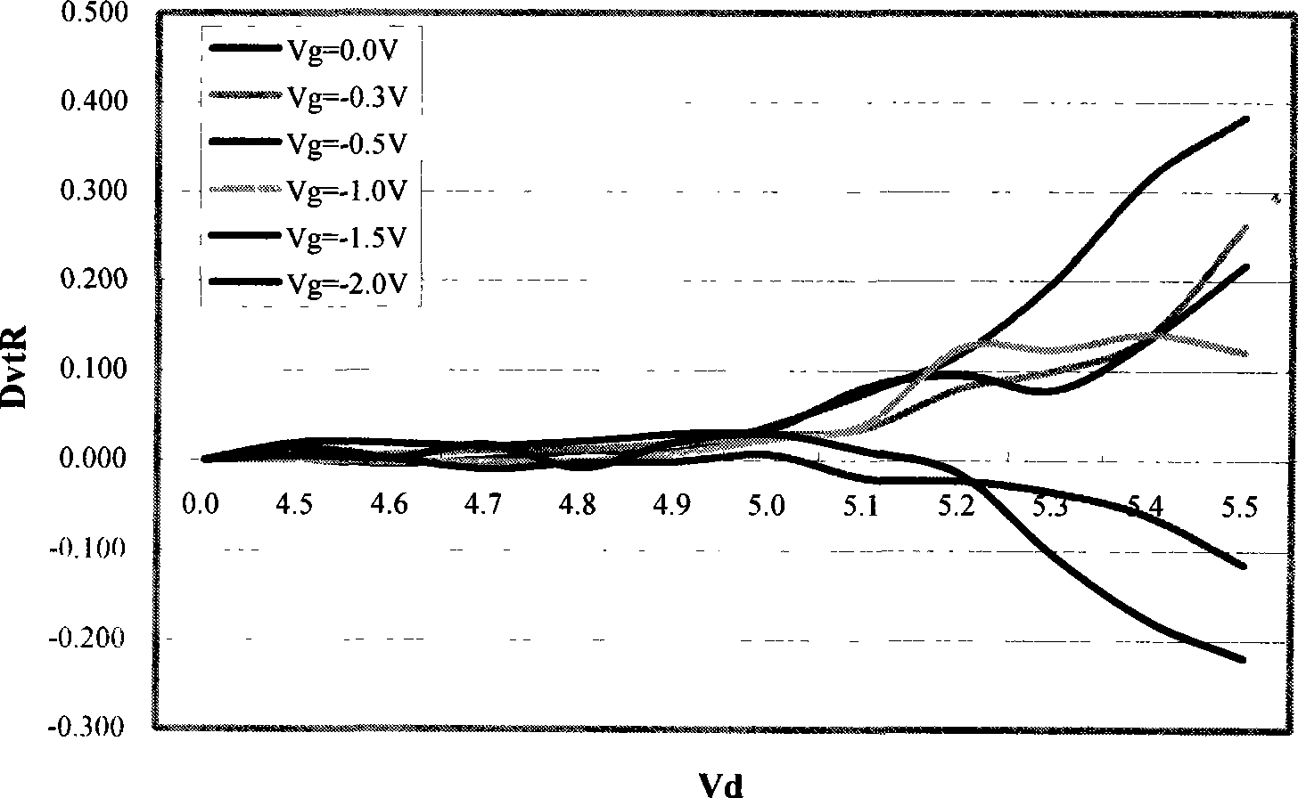
[0019] In order to determine the best bias voltage value, taking the memory cell C21 as an example, the following experiments were carried out on its unp...


PUM


Abstract

The invention discloses a method for preventing a memory array from generating bit line interference. The memory array consists of a plurality of storage units which are in array management, wherein each storage unit comprises a grid, a source electrode, and a drain electrode. The grids of the storage units in each row are connected to form a straight line. The source electrodes and the drain electrodes of the storage units of each row are connected to a bit line. Two adjacent storage units share a bit line. According to the method, when a certain storage unit is programmed, and if two bit lines connected to the other storage units are in high potential, and one bit line connected thereto is in suspension state or in low potential, a grid bias voltage is loaded to the other storage units. The method of the invention can prevent the nonvolatile memory from generating bit line interference, thereby improving the performance of the memory.

Description

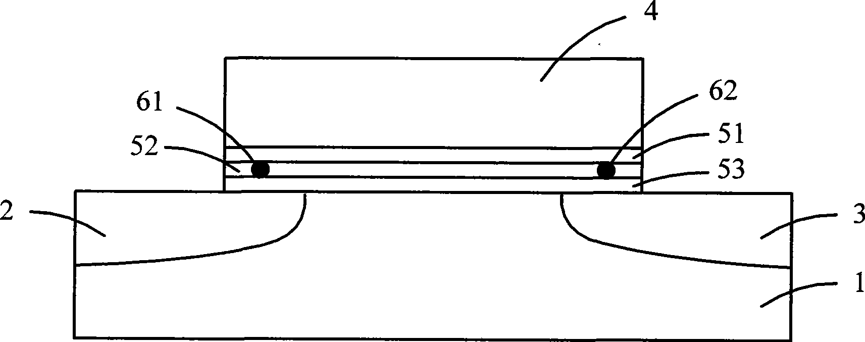
technical field [0001] The invention relates to the erasing and writing technology of data of semiconductor devices, in particular to a method for preventing bit line interference from non-volatile memory arrays. Background technique [0002] Nonvolatile memory (nonvolatile memory) is a commonly used semiconductor device. According to different materials and structures, nonvolatile memory can be divided into many types. Taking nitrogen read-only memory (NROM) as an example, it has such figure 1 The device structure shown includes: a substrate 1, a source 2 and a drain 3 formed in the substrate 1, and a gate 4 formed above the substrate 1, wherein, between the gate 4 and the substrate 1 There are also three superimposed insulating layers 51, 52, 53 between them, the middle layer 52 is a charge-trapping layer for storing data, and the insulating layers 51, 53 on the upper and lower sides are used to lock the middle Layer 52 charges. Two ends of the charge trapping layer 52 ...

Claims


Application Information

Patent Timeline
Patent Type & Authority Applications(China)
IPC IPC(8): G11C16/10
Inventor 缪威权陈良成刘鉴常蔡恩静易晶晶陈德艳
Owner SEMICON MFG INT (SHANGHAI) CORP
Learn More