

Method for preventing memory array generating bit line interference
A memory array and bit line technology, applied in static memory, read-only memory, information storage, etc., can solve the problems of memory cell interference, increase of threshold voltage variation DVt, and influence on memory cell performance, so as to reduce potential difference, Improving the Effect of Bit Line Disturbance
- Summary
- Abstract
- Description
- Claims
- Application Information
AI Technical Summary
Problems solved by technology
Method used
Image

Examples
Embodiment Construction
[0017] The method for preventing bit line interference in the memory array of the present invention will be described in further detail below.
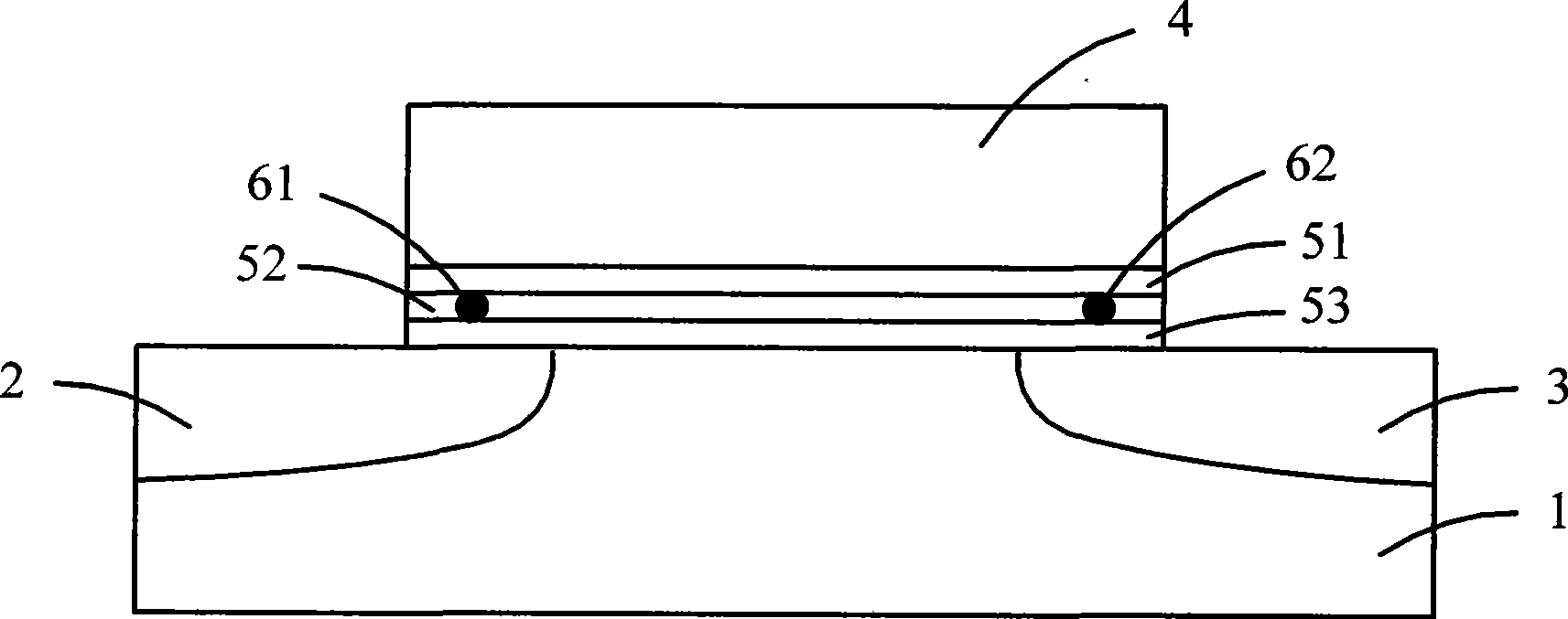
[0018] The method of the present invention is that when a memory cell is being programmed, if one of the two bit lines connected to the adjacent memory cell is at a high potential, the other is at a floating state or a low potential, that is, there is a gap between the source and the drain. When the potential is different, a gate bias voltage Vg is applied to the memory cell.
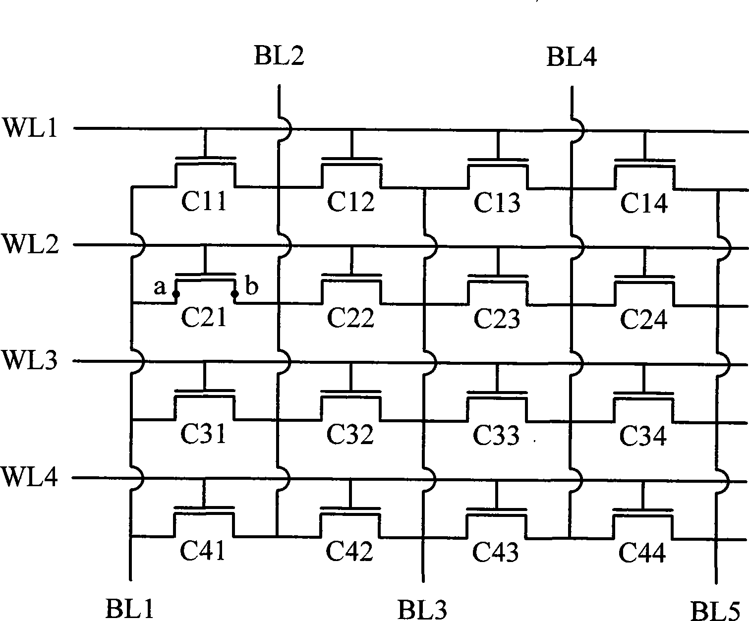
[0019] See figure 2 For example, when the memory cell C11 is receiving programming, the bit line BL2 is at a high potential, the bit line BL1 is at a low potential, and the bit line BL3 is in a floating state. At this time, the memory cells C21 and C22 are disturbed and need to be The gate bias voltage Vg is applied.
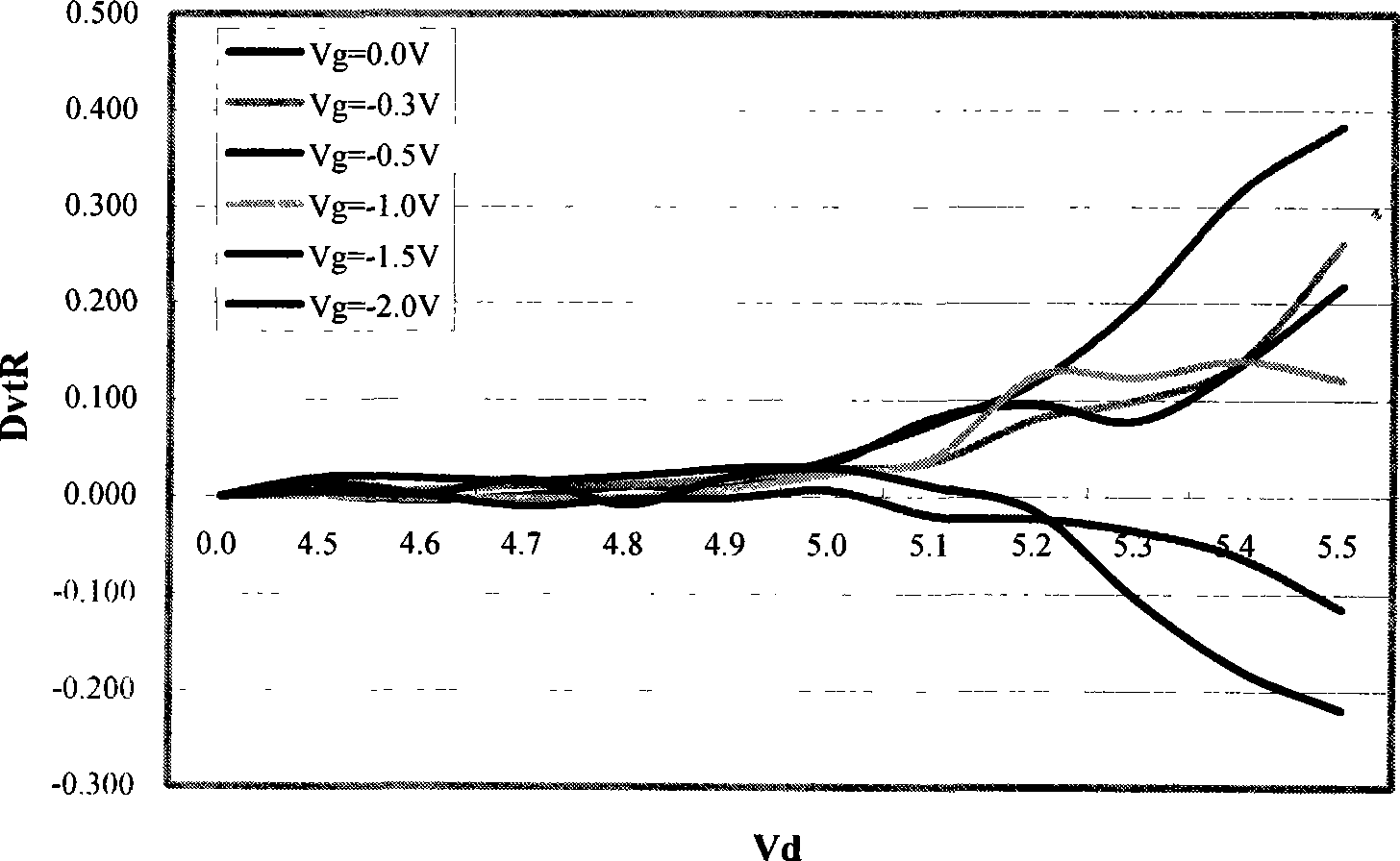
[0020] In order to determine the best bias voltage value, take the memory cell C21 as an example, the following experiments were carried out for its ...
PUM
 Abstract
Description
Claims
Application Information