

Nonvolatile semiconductor memory device
A storage device, non-volatile technology, applied in the direction of semiconductor devices, semiconductor/solid-state device manufacturing, information storage, etc., can solve the problems of unusable reliability, deterioration of charge retention characteristics, and non-negligible charging loss bits, etc., to achieve stability discrete small effects
- Summary
- Abstract
- Description
- Claims
- Application Information
AI Technical Summary
Problems solved by technology
Method used
Image

Examples
Embodiment 1
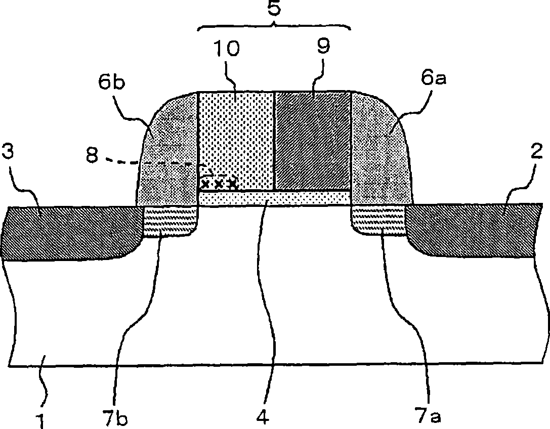
[0060] A nonvolatile semiconductor memory device according to Embodiment 1 of the present invention will be described with reference to the drawings. figure 1 It is a partial cross-sectional view schematically showing the configuration of the nonvolatile semiconductor memory device according to Embodiment 1 of the present invention.
[0061] figure 1 The non-volatile semiconductor storage device is Nch type, and N+ type source 2 and drain 3 are formed on the surface of P-type semiconductor substrate 1 (also can be P well), and between source 2 and drain 3 A gate electrode 5 is formed on the intermediate semiconductor substrate 1 via a gate insulating film 4 (for example, a silicon oxide film). A part of the gate electrode 5 becomes the non-doped region 10 (such as polysilicon), and the other region of the gate electrode 5 becomes the doped region 9 (such as N+polysilicon). exist figure 1 Among them, the portion of the gate electrode 5 on the drain 3 side serves as the un...
Embodiment 2
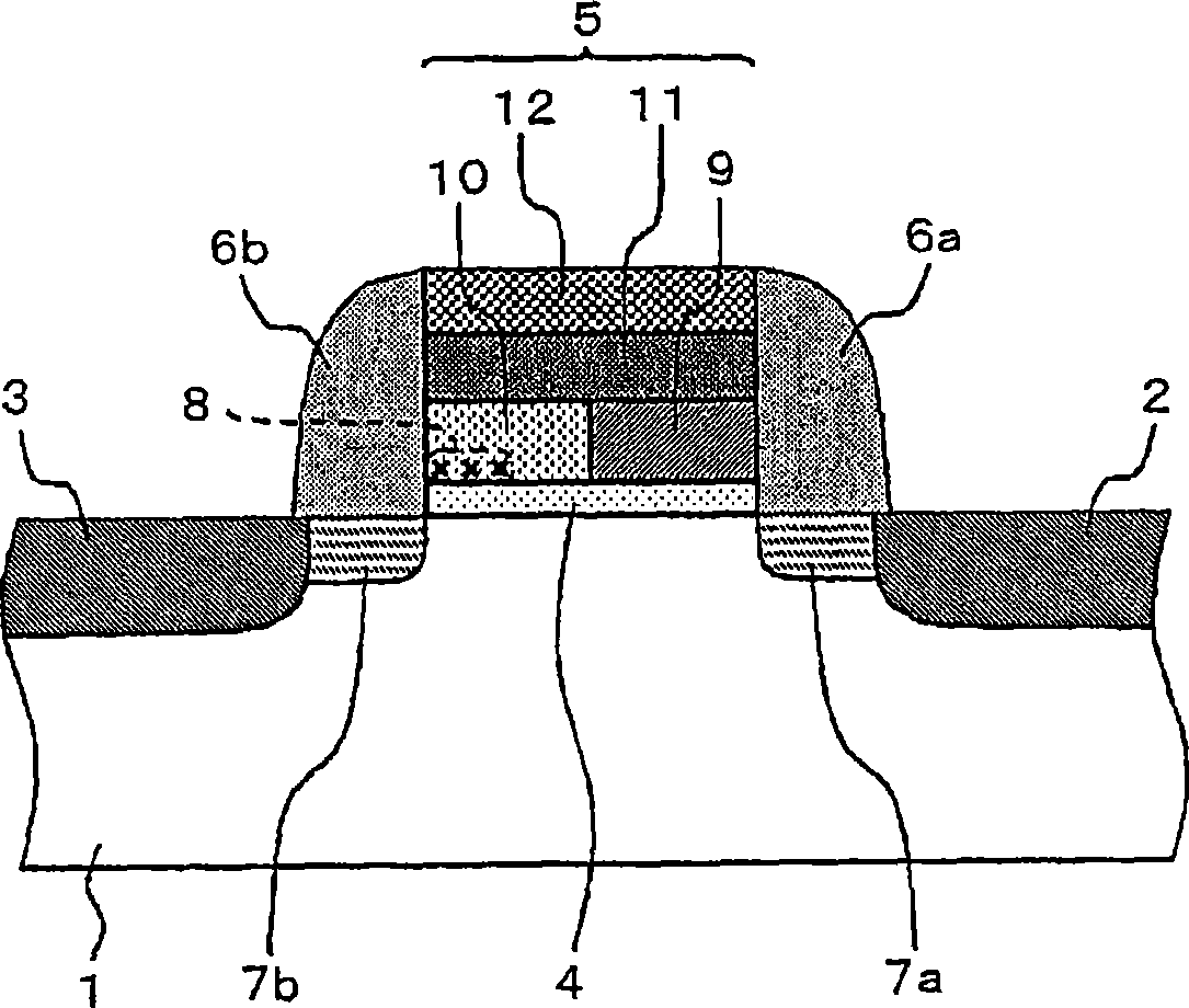
[0072] A nonvolatile semiconductor memory device according to Embodiment 2 of the present invention will be described with reference to the drawings. figure 2 It is a partial cross-sectional view schematically showing the configuration of the nonvolatile semiconductor memory device according to Embodiment 2 of the present invention.
[0073] The configuration of the gate electrode 5 in the nonvolatile semiconductor memory device of the second embodiment is different from that of the first embodiment. The gate electrode 5 is composed of a polysilicon layer, a silicide layer 11, The metal layer 12 is formed. A portion of the polysilicon layer on the drain 3 side serves as an undoped region 10 , and a portion of the polysilicon layer on the source 2 side serves as a doped region 9 . In addition, the metal layer 12 may not be included in the gate electrode 5, and only a polysilicon layer and a silicide layer having the doped region 9 and the non-doped region 10 may be laminated...
Embodiment 3
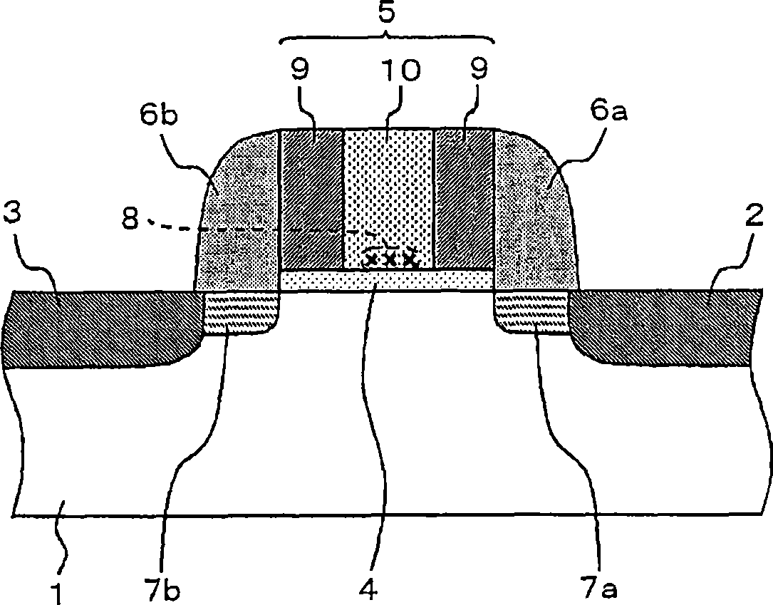
[0077] A nonvolatile semiconductor memory device according to Embodiment 3 of the present invention will be described with reference to the drawings. image 3 It is a partial sectional view schematically showing the configuration of the nonvolatile semiconductor memory device according to Embodiment 3 of the present invention.
[0078] The configuration of the gate electrode 5 in the nonvolatile semiconductor memory device of the third embodiment is different from that of the first embodiment. Portions of the gate electrode 5 on the side of the drain 3 and the side of the source 2 serve as the doped region 9 (N+ polysilicon), and the central part of the gate electrode 5 serves as the non-doped region 10 (polysilicon). Other configurations and actions are the same as those in Embodiment 1. Also, it is also possible to apply the configuration of the gate electrode 5 as in Embodiment 3 to the polysilicon layer ( figure 2 9, 10 of the layer).
[0079] According to Example 3, t...
PUM
 Abstract
Description
Claims
Application Information