Multilayer printed wiring board and method for fabrication thereof

A technology of multi-layer printing and production method, applied in the direction of multi-layer circuit manufacturing, printed circuit manufacturing, printed circuit, etc., can solve problems such as disadvantages, and achieve the effect of preventing connection deterioration, damage and deformation

Inactive Publication Date: 2009-04-01
SHARP KK
View PDF1 Cites 9 Cited by
  • Summary
  • Abstract
  • Description
  • Claims
  • Application Information

AI Technical Summary

Problems solved by technology

However, doing so would disadvantageously require an additional process of forming a reinforcing piece in the terminal portion

Method used


Image

  • Multilayer printed wiring board and method for fabrication thereof
  • Multilayer printed wiring board and method for fabrication thereof
  • Multilayer printed wiring board and method for fabrication thereof

Examples


no. 1 approach

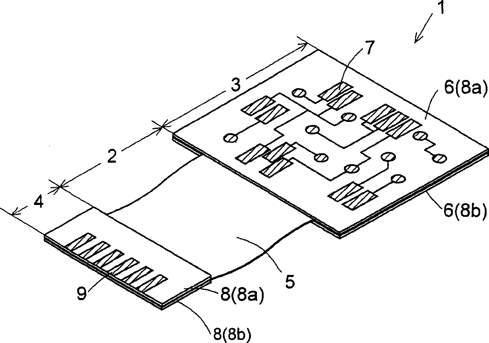
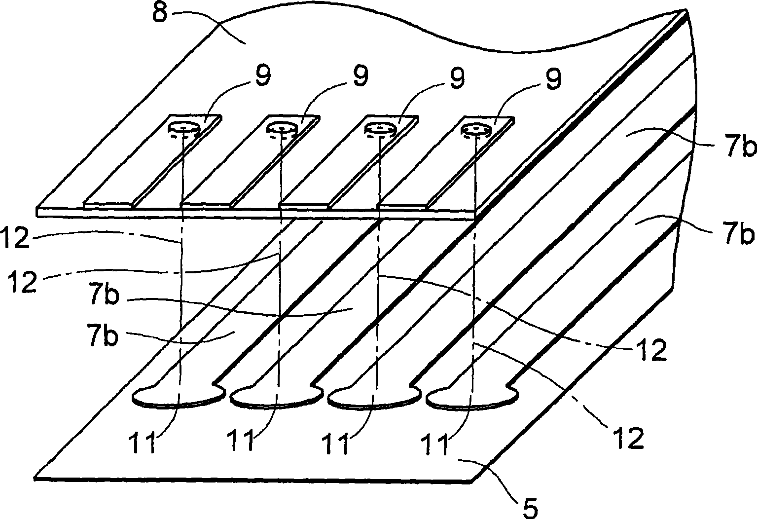
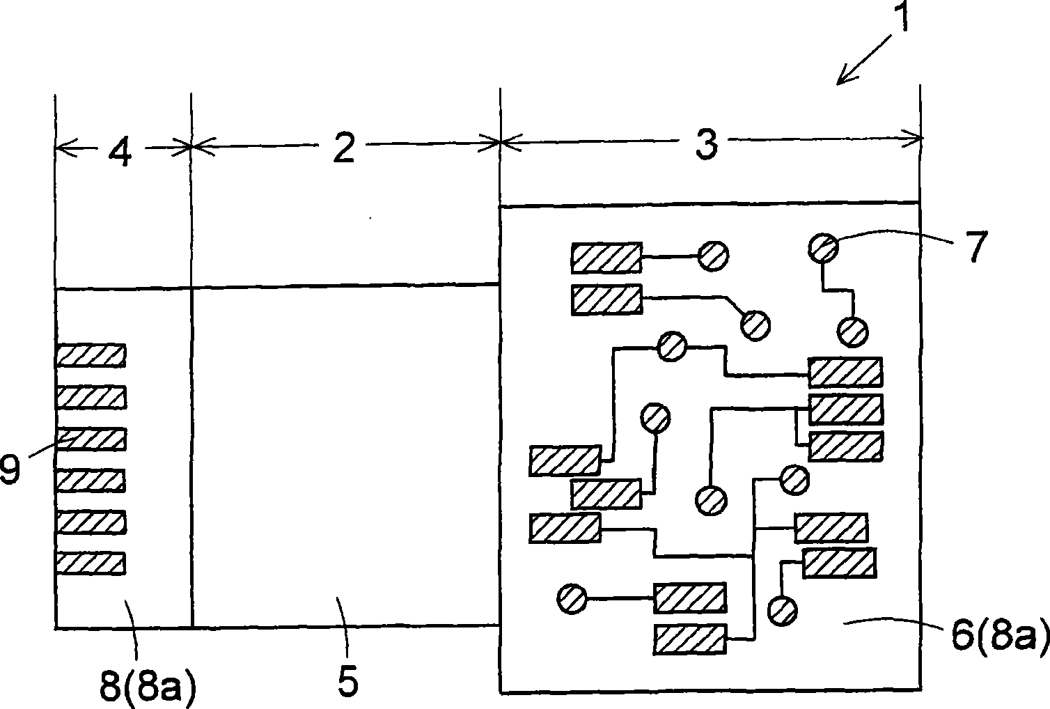
[0059] Figures 1 to 6 The structure of the multilayer printed wiring board according to the first embodiment of the present invention is shown. A multilayer printed wiring board having four conductor layers in total and including a terminal portion having two conductor layers will be described. However, the number of conductor layers formed is not limited to those described above; any number of conductor layers may be formed. The present invention is applicable to any type of multilayer printed wiring board as long as it is provided with a terminal portion.

[0060] The multilayer printed wiring board 1 of the first embodiment is configured as a so-called rigid-flexible wiring board. Specifically, as figure 1 As shown, a multilayer printed wiring board 1 is composed of a flexible portion 2 , a rigid portion 3 and a terminal portion 4 . The flexible portion 2 is configured as a flexible printed wiring board 5 formed of a thin material. The rigid part 3 is formed by formin...

no. 2 approach

[0078] Figure 14 and 15 A multilayer printed wiring board 101 according to a second embodiment of the present invention is shown. For the convenience of description, the same reference numerals are used to denote the Figures 1 to 13 Those of the first embodiment shown have corresponding parts, and descriptions thereof are omitted. A multilayer printed wiring board having six conductor layers in total and including a terminal portion having two conductor layers will be described. However, the number of conductor layers formed is not limited to those described above; any number of conductor layers may be formed. The present invention is applicable to any other type of multilayer printed wiring board as long as it is provided with a terminal portion.

[0079] Such as Figure 14 As shown, the multilayer printed wiring board 101 of the second embodiment is composed of a flexible portion 2 , a rigid portion 3 and a terminal portion 4 . The flexible portion 2 is configured as...

no. 3 approach

[0091] Figure 19 and 20 A multilayer printed wiring board according to a third embodiment of the present invention is shown. For the convenience of description, the same reference numerals are used to denote the Figures 1 to 18 Those parts in the first and second embodiments shown have corresponding parts, and descriptions thereof are omitted.

[0092] Such as Figure 19 As shown, the multilayer printed wiring board 201 of the third embodiment is composed of a flexible portion 2 , a rigid portion 3 , and a terminal portion 4 . The flexible portion 2 is configured as a flexible printed wiring board 5 . The rigid portion 3 is configured by forming a rigid portion 202 and a wiring layer 203 on a part of both surfaces of the flexible printed wiring board 5 . The terminal portion 4 is removed from the flexible printed wiring board 5 by forming an insulating layer 204 on both surfaces of the end portion of the flexible printed wiring board 5 so that a part of the insulating l...


PUM


Abstract

Provided is a multilayer printed wiring board having a terminal portion of high quality. This multilayer printed wiring board 1 has a flexible portion 2 having flexibility, the flexible portion 2 that can be bent when used, a rigid portion 3 formed continuously with the flexible portion, the rigid portion 3 having greater rigidity than the flexible portion 2, and a terminal portion 4 formed continuously with the flexible portion 2 at an end portion of the flexible portion. The rigid portion 3 includes a rigid layer 6 having insulation properties. The terminal portion 4 includes an insulating layer 8 formed of the same material as that for the rigid layer 6, the insulating layer 8 having a conductive layer 9 formed on the surface thereof, the conductive layer 9 having a predetermined terminal pattern and serving as a connecting terminal.

Description

technical field [0001] The present invention relates to a multilayer printed wiring board and its manufacturing method. Background technique [0002] Conventionally, a multilayer printed wiring board called a rigid-flexible wiring board is known. In general, a rigid-flexible wiring board (multilayer printed wiring board) consists of a part that is flexible and mainly used as a cable (hereinafter "flexible part") and a part that is rigid (hereinafter "rigid part"). ”) configuration, high-density wiring is possible in the rigid part and operations such as mainly mounting electronic parts are performed. This structure allows a rigid-flexible wiring board (multilayer printed wiring board) to be used with the flexible portion bent, making it possible to effectively utilize a small mounting area regardless of the electronic parts that need to be mounted in the case of electronic device miniaturization. fact on smaller installation area. [0003] The above-mentioned multilayer p...

Claims


Application Information

Patent Timeline
Patent Type & Authority Applications(China)
IPC IPC(8): H05K3/46H05K1/02
CPCH05K1/148H05K3/4652H05K2201/2009H05K1/117H05K2201/09481H05K3/4691H05K2201/0715H05K2201/0949H05K2201/09127Y10T29/49147
Inventor 上野幸宏
Owner SHARP KK
Why Eureka
Try Eureka