
Wireless IC device

一种集成电路、无线的技术,应用在电路、天线、天线端点间的中间位置馈电等方向,能够解决天线增益小、难以实现阻抗匹配、天线小等问题,达到提高天线增益的效果

Active Publication Date: 2009-04-22
MURATA MFG CO LTD
View PDF2 Cites 8 Cited by
  • Summary
  • Abstract
  • Description
  • Claims
  • Application Information

AI Technical Summary

Problems solved by technology

However, since the wireless integrated circuit chip itself is very small, the antenna formed on the chip is also very small, and the gain of the antenna is very small.
However, in this configuration, since the antenna on the substrate side is a closed loop, sufficient gain can be obtained in a low frequency band such as 13.56 MHz, but once it reaches a frequency band above the ultra high frequency (UHF) band, wireless integrated It is difficult to achieve impedance matching between the antenna coil on the circuit chip side and the antenna on the substrate side

Method used


Image

  • Wireless IC device
  • Wireless IC device
  • Wireless IC device

Examples


no. 1 Embodiment

[0048] (for the first embodiment, refer to figure 1 )

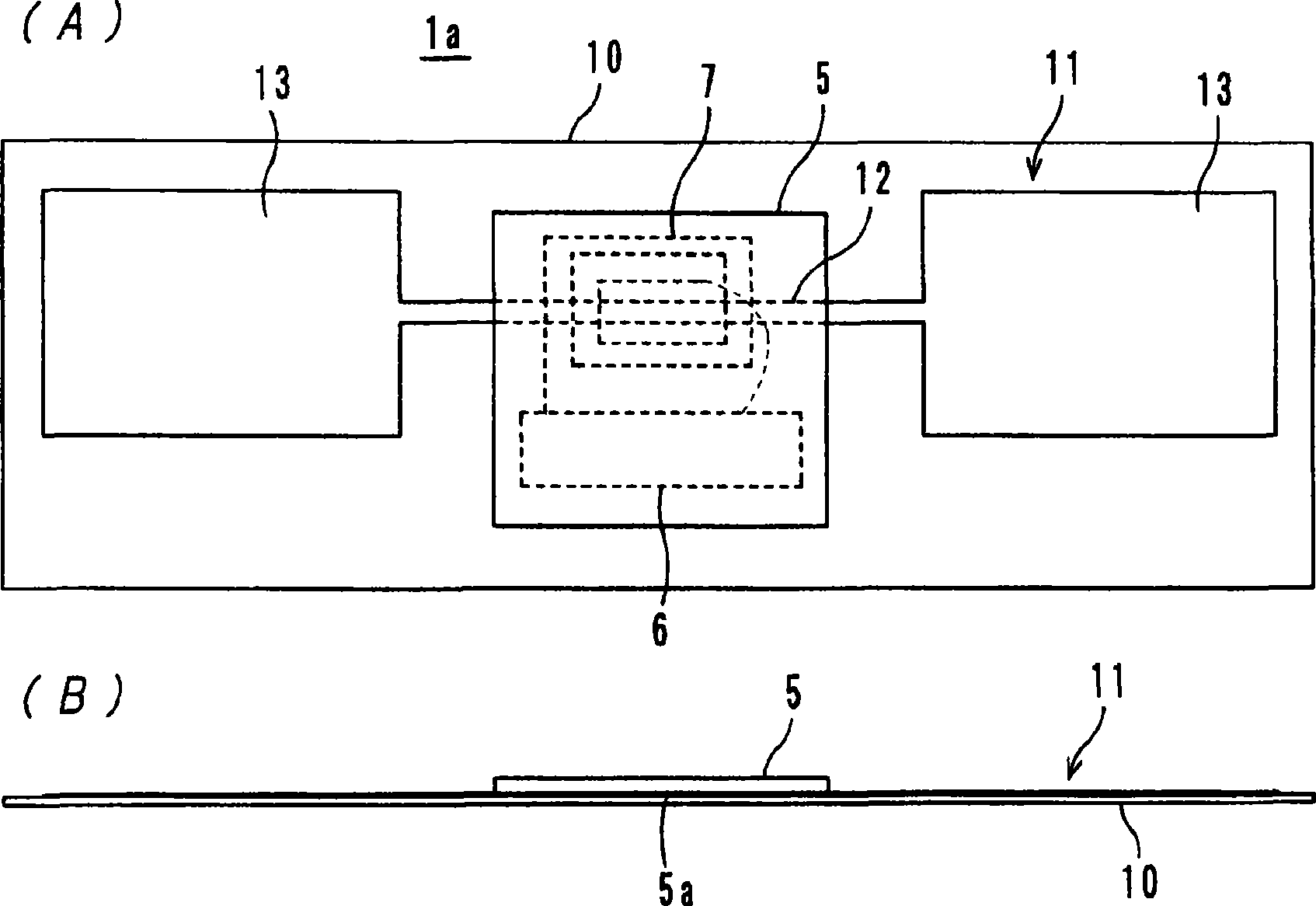
[0049] The wireless integrated circuit device 1a of the first embodiment, such as figure 1 (A), shown in (B), form radiation board 11 on support film 10, on the upper surface of support film 10, namely the power supply part 12 of radiation board 11, wireless integrated circuit chip 5 is pasted on it with adhesive. superior. The radiation plate 11 is a double-sided open type (both open type) composed of a linear feeding portion 12 and a large-area radiation portion 13 . The radiation plate 11 is made of a flexible aluminum foil or a metal film formed by metal vapor deposition, and the support film 10 is made of an insulating flexible film such as polybutylene terephthalate (PET). In addition to films, paper or synthetic paper can also be used.

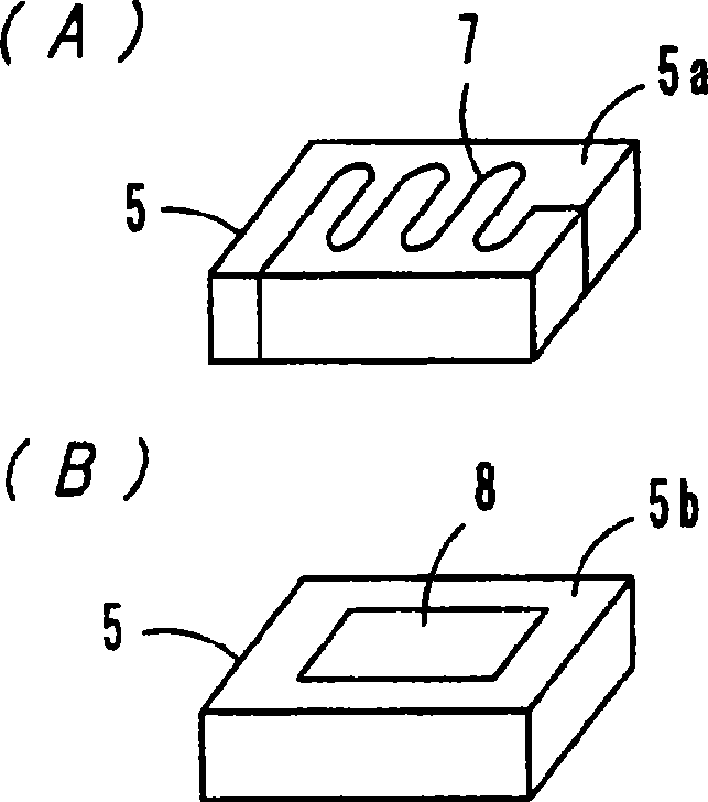
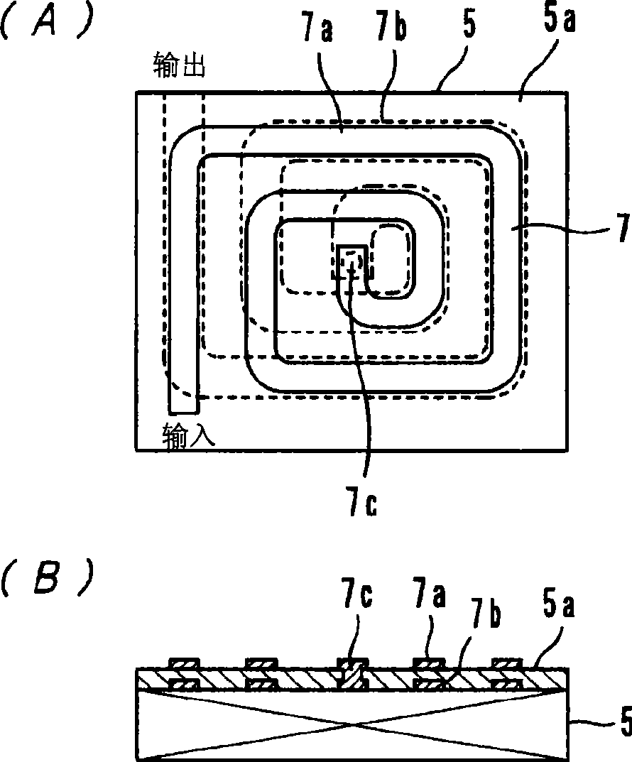
[0050] The wireless integrated circuit chip 5 incorporates a signal processing unit 6 , and a power supply circuit 7 formed of a coil-shaped electrode pattern is formed on the ...

no. 2 Embodiment

[0063] (for the second embodiment, refer to Figure 5 )

[0064] As the wireless integrated circuit device 1b of the second embodiment, such as Figure 5 As shown, on the supporting film 10, metal films such as aluminum foil or metal vapor-deposited film are used to form a cross-shaped power supply part 12 and large radiation beams respectively extending in the x direction and the y direction connected to the two ends of the power supply part 12. The radiating plate 11 composed of part 13 is attached to the support film 10 with an adhesive to stick the wireless integrated circuit chip 5 so that the center of the power supply circuit 7 coincides with the intersection point of the power supply part 12. In addition, it is preferable that the center of the power supply circuit 7 coincides with the intersection point of the power supply part 12, but it does not matter if there is some deviation.

[0065] The operation and effect of this wireless integrated circuit device 1b are t...

no. 3 Embodiment

[0066] (the 3rd embodiment, refer to Figure 6 ~ Figure 8 )

[0067] The wireless integrated circuit device 1c of the third embodiment is such as Image 6 As shown, a power supply circuit 7 composed of two coil-shaped electrode patterns is arranged inside the wireless integrated circuit chip 5, and the linear power supply part 12 of the radiation plate 11 is arranged between the power supply circuits 7.

[0068] Figure 7 Shown is a wireless integrated circuit device 1c' as a modified example. The power supply circuit 7 of the wireless integrated circuit chip 5 of the wireless integrated circuit device 1c' is formed with two meandering electrode patterns, and the other structures are the same as the wireless integrated circuit device 1c. In addition, the winding direction can be horizontal or vertical.

[0069] The functions and effects of the wireless integrated circuit devices 1c, 1c' are the same as those of the first embodiment. That is, the high-frequency signal (suc...


PUM


Abstract

Provided is a wireless IC device having a large antenna gain, operable at a sufficient distance from a reader / writer, and sufficiently usable even at frequencies above the UHF band. The wireless IC device comprises a wireless IC chip (5) having a feeder circuit (7) including a resonant circuit with a predetermined resonant frequency and a radiation plate (11) for radiating a transmission signal supplied from the feeder circuit (7) to the outside and also supplying a signal received from the outside to the feeder circuit (7). The radiation plate (11) and the feeder circuit (7) are coupled witheach other through electric field or magnetic field. The radiation plate (11) is a both-side open type having radiation portions (13) for exchanging transmitting and receiving signals with the outside and a feed portion (12) for exchanging the transmitting and receiving signals with the feeder circuit (7).

Description

technical field [0001] The present invention relates to wireless integrated circuit devices, and more particularly to wireless integrated circuit devices for radio frequency identification (RFID) systems. Background technique [0002] In recent years, as a management system for items, research is being conducted on radio frequency tags that enable non-contact communication between a reader-writer that generates an induced electromagnetic field and an integrated circuit tag (hereinafter referred to as a wireless integrated circuit device) that stores specified information attached to an item, and transmits information. recognition system. Wireless integrated circuit devices used in radio frequency identification systems are generally formed with winding coils formed by etching or printing on a substrate carrying wireless integrated circuit chips. [0003] On the other hand, Patent Document 1 discloses a wireless integrated circuit device in which an antenna coil is formed by...

Claims


Application Information

Patent Timeline
Patent Type & Authority Applications(China)
IPC IPC(8): H01Q23/00H01Q1/38G06K19/07H01Q9/28G06K19/077H01Q13/08H01Q1/22H01Q21/08
CPCH01Q9/28H01Q21/08H01Q23/00H01Q1/2208G06K19/07749G06K19/07786H01Q1/38H01Q21/24
Inventor 加藤登
Owner MURATA MFG CO LTD
Learn More