Flash memory recognition method, recognition device and chip controller

A memory identification and memory technology, applied in static memory, instrument, etc., can solve the problems that FLASH memory cannot be used, it is difficult to include conversion information of FLASH memory, and the key parameters of command data decoder are limited, etc.

Inactive Publication Date: 2009-04-29
VIMICRO CORP
View PDF3 Cites 22 Cited by
  • Summary
  • Abstract
  • Description
  • Claims
  • Application Information

AI Technical Summary

Problems solved by technology

[0007] But, the shortcoming of this mode is, the key parameter that command data decoder 13 can store in advance is very limited, it is difficult to all include the conversion information of the FLASH memory that all manufacturers produce, and, the speed of FLASH memory update is very fast, if control If there is no corresponding configuration information for the new product in the device, the FLASH memory will be unusable

Method used


Image

  • Flash memory recognition method, recognition device and chip controller
  • Flash memory recognition method, recognition device and chip controller
  • Flash memory recognition method, recognition device and chip controller

Examples


Embodiment Construction

[0035] In order to make the above objects, features and advantages of the present invention more comprehensible, the present invention will be further described in detail below in conjunction with the accompanying drawings and specific embodiments.

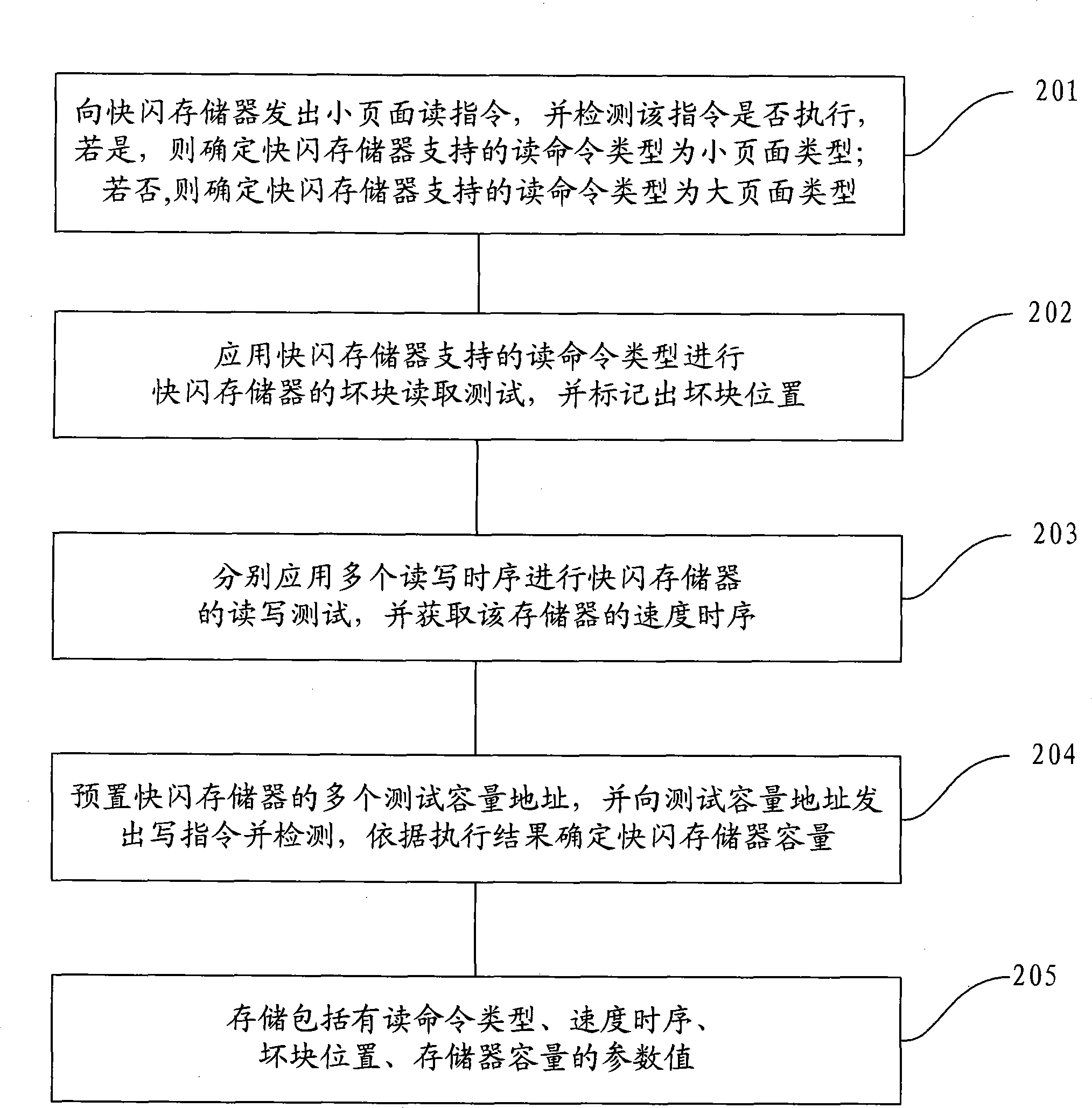
[0036] refer to figure 2 , shows a flow chart according to an embodiment of the flash memory identification method of the present invention, after the flash memory is powered on and reset, the following steps are performed:

[0037] Step 201: Send a small page read instruction to the flash memory, and check whether the instruction is executed, if so, determine that the type of read command supported by the flash memory is a small page type; if not, determine that the flash memory The read command type supported by the memory is a large page type;

[0038] Step 202: Apply the read command type supported by the flash memory to perform a bad block reading test of the flash memory, and mark the location of the bad block;

[0039] S...


PUM


Abstract

The invention provides a recognition method of a flash memory, identification equipment thereof and a chip controller; wherein, the recognition method of the flash memory comprises the steps: the page types supported by the flash memory are judged, the positions of bad blocks are determined, the speed time sequence of the memory is acquired; the capacity of the memory is obtained, and a plurality of key parameters of the flash memory are obtained in a self-adapting way, thereby the chip controller can realize to control the flash memory according to the identified key parameters under the condition that a data decoder of a control chip does not store the key parameters of the flash memory connected with the chip controller.

Description

technical field [0001] The invention relates to the field of flash memory, in particular to a flash memory identification method, an identification device, and a chip controller. Background technique [0002] NAND flash memory (NAND FLASH) is a non-volatile semiconductor memory that can be electrically erased online. It has the advantages of fast erase and write speed, low power consumption, large capacity, and low cost. It is widely used in MP3, MP4, In electronic products such as mobile phones, digital cameras, and video cameras. The NAND FLASH chip writes and reads data through the NAND FLASH controller, and the data transmitted by the NAND FLASH controller to the NAND FLASH chip includes address data, command data and information data. The existing NAND FLASH controller transmits address, command data, and information data to the NAND FLASH memory through an internal data transmission channel. [0003] refer to figure 1 , is a schematic structural diagram of an existi...

Claims


Application Information

Patent Timeline
Patent Type & Authority Applications(China)
IPC IPC(8): G11C29/44
Inventor 张浩
Owner VIMICRO CORP
Why Eureka
Try Eureka