Method for preparing compound semiconductor substrate

A technology of semiconductors and compounds, applied in semiconductor/solid-state device manufacturing, electrical components, circuits, etc., can solve the problems of increasing processing time and processing costs

Active Publication Date: 2009-05-20
硅得荣株式会社
View PDF0 Cites 3 Cited by
  • Summary
  • Abstract
  • Description
  • Claims
  • Application Information

AI Technical Summary

Problems solved by technology

However, silicon substrates are also limited in that it is difficult to form high-quality GaN epitaxial layers on them.
[0013] As mentioned above, while the ma

Method used


Image

  • Method for preparing compound semiconductor substrate
  • Method for preparing compound semiconductor substrate
  • Method for preparing compound semiconductor substrate

Examples


Embodiment Construction

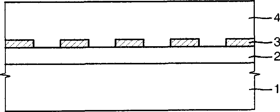
[0027] Hereinafter, specific embodiments will be described in detail with reference to the accompanying drawings. However, this invention may be embodied in different forms and should not be construed as limited to the embodiments set forth herein. Rather, these embodiments are provided so that this disclosure will be thorough and complete, and will fully convey the scope of the invention to those skilled in the art. In the drawings, the shapes of elements are exaggerated for clarity of illustration, and like reference numerals refer to like elements throughout. Those skilled in the art will appreciate that when an element such as a layer is referred to herein as being "on / under" another element, that element can be directly on / under the other element, and one or more intervening elements may also be present. .

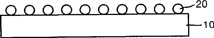
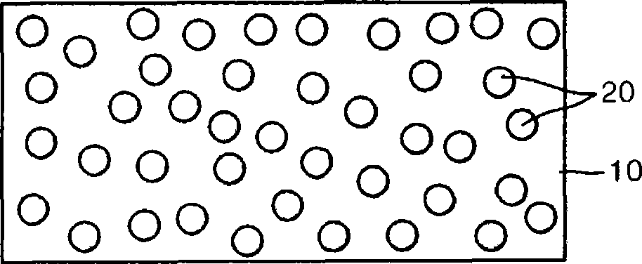
[0028] Embodiments of the present invention focus primarily on on-substrate sphere processing. The sphere treatment reduces dislocations equally or more effectivel...


PUM


Abstract

Provided is a method for preparing a compound semiconductor substrate. The method includes coating a plurality of spherical balls on a substrate, growing a compound semiconductor epitaxial layer on the substrate coated with the spherical balls while allowing voids to be formed under the spherical balls, and cooling the substrate on which the compound semiconductor epitaxial layer is grown so that the substrate and the compound semiconductor epitaxial layer are self-separated along the voids. The spherical ball treatment can reduce dislocation generations. In addition, because the substrate and the compound semiconductor epitaxial layer are separated through the self-separation, there is no need for laser lift-off process.

Description

technical field [0001] The present invention relates to a compound semiconductor layer formed of gallium nitride (GaN) or a nitride of gallium and other metals and a method for forming the compound semiconductor layer. The invention also relates to a method for preparing a substrate used in the manufacture of electronic or photo-electronic devices comprising compound semiconductor layers. The present invention relates to the technical field for forming a high-quality compound semiconductor layer on a substrate, and more particularly, to the technical field for preparing a free-standing compound semiconductor substrate by separating the substrate from the compound semiconductor layer. Background technique [0002] Semiconductor materials based on nitrides of Group III elements or Group V elements have already occupied an important position in the fields of electronics and optoelectronics, and will become more and more important. In fact, nitride-based semiconductor materials...

Claims


Application Information

Patent Timeline
IPC IPC(8): H01L21/02H01L21/20
CPCH01L21/02639H01L21/0242H01L21/02664H01L21/0254H01L21/02642H01L21/02378H01L21/02381H01L21/20
Inventor 李浩准金容进李东键金杜洙金知勋
Owner 硅得荣株式会社
Why Eureka
Try Eureka