

Method for epitaxial growth of ultraviolet LED with high luminous efficacy
A technology of epitaxial growth and high light efficiency, applied in electrical components, circuits, semiconductor devices, etc., can solve the problems of high preparation cost, difficulty and low yield, and achieve the effect of increasing radiation power and reducing the difficulty of growth.
- Summary
- Abstract
- Description
- Claims
- Application Information
AI Technical Summary
Problems solved by technology
Method used
Image

Examples
Embodiment 1
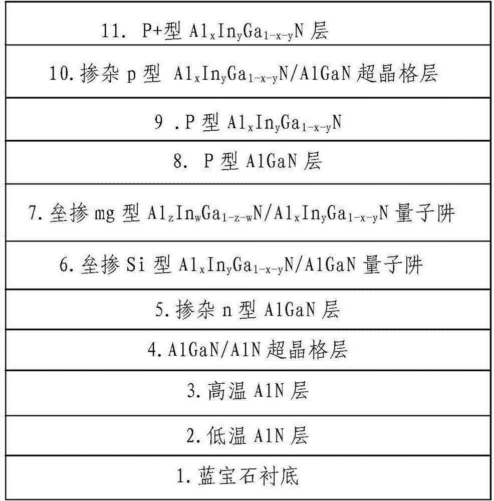
[0052] 1. After cleaning the sapphire substrate, put it into the MOCVD equipment and bake it at 1100°C for 10 minutes.
[0053] 2. A low-temperature AlN layer with a thickness of 10 nm is grown at a temperature of 600° C., and the growth pressure is 200 torr.
[0054] 3. Raise the temperature to 1070°C to grow an intrinsic AlN layer with a thickness of 300nm, and the growth pressure is 200torr.
[0055] 4. A layer of 10-period AlN / AlGaN superlattice is grown at a temperature of 1050° C. and 200 torr, with a total thickness of 70 nm.
[0056] 5. Grow a silane-doped n-type AlGaN layer at a temperature of 1050°C with a thickness of 500nm and a pressure of 200torr.
[0057] 6. Grow a 3nm AlxInyGa1-x-yN layer at 850°C in a nitrogen atmosphere of 50torr; then raise the temperature to 950°C and 200torr to grow a 12nm AlGaN layer, doping a small amount of silane during the growth process; then repeat the growth of 3 cycle.
[0058] 7. Then grow a layer of about 3nm Al in nitrogen a...
Embodiment 2
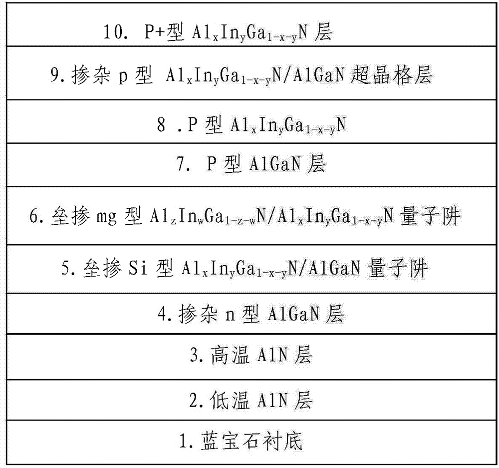
[0067] 1. After cleaning the sapphire substrate, put it into the MOCVD equipment and bake it at 1100°C for 10 minutes.
[0068] 2. A low-temperature AlN layer with a thickness of 10 nm is grown at a temperature of 600° C., and the growth pressure is 200 torr.
[0069] 3. Raise the temperature to 1070°C to grow an intrinsic AlN layer with a thickness of 300nm, and the growth pressure is 200torr.
[0070] 4. Grow a silane-doped n-type AlGaN layer with a thickness of 500nm at a temperature of 1050°C and a pressure of 200torr.
[0071] 5. Grow a layer of about 3nm Al in nitrogen atmosphere 50torr, 850℃ x In y Ga 1-x-y N layer; then raise the temperature to 950°C and 200torr, and then grow a 12nm AlGaN layer, doped with a small amount of silane during the growth process; then repeat the growth for 3 cycles.
[0072] 6. Then grow a layer of about 3nm Al in nitrogen atmosphere 50torr, 850℃ x In y Ga 1-x-y N layer, followed by a layer of Al z In w Ga 1-z-w N(x<z<1, w<y<1, 0<...
Embodiment 3
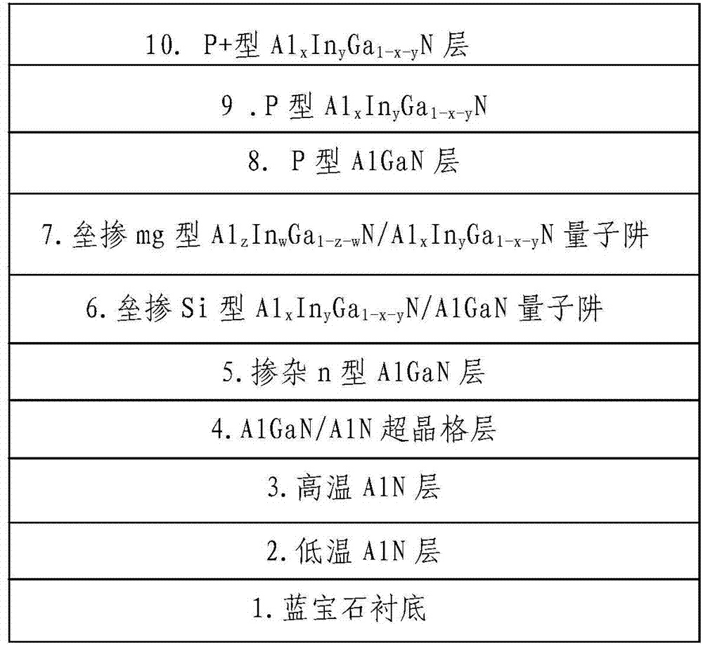
[0081] 1. After cleaning the sapphire substrate, put it into the MOCVD equipment and bake it at 1100°C for 10 minutes.
[0082] 2. A low-temperature AlN layer with a thickness of 10 nm is grown at a temperature of 600° C., and the growth pressure is 200 torr.
[0083] 3. Raise the temperature to 1070°C to grow an intrinsic AlN layer with a thickness of 300nm, and the growth pressure is 200torr.
[0084] 4. A layer of 10-period AlN / AlGaN superlattice is grown at a temperature of 1050° C. and 200 torr, with a total thickness of 70 nm.
[0085] 5. Grow a silane-doped n-type AlGaN layer with a thickness of 500nm at a temperature of 1050°C and a pressure of 200torr.
[0086] 6. Grow a layer of about 3nm Al in a nitrogen atmosphere of 50torr and 850℃ x In y Ga 1-x-y N layer; then raise the temperature to 950°C and 200torr, and then grow a 12nm AlGaN layer, doped with a small amount of silane during the growth process; then repeat the growth for 3 cycles.
[0087] 7. Then grow a...
PUM
 Abstract
Description
Claims
Application Information