Thermal field structure for drawing zone-melting 8-12-inch silicon single crystal

A silicon single crystal, drawing area technology, applied in the direction of single crystal growth, single crystal growth, self-regional melting method, etc., can solve the problems of generator power increase, ionization breakdown, thermal stress increase, etc.

Pending Publication Date: 2015-12-30
TIANJIN ZHONGHUAN ADVANCED MATERIAL TECH
View PDF4 Cites 0 Cited by
  • Summary
  • Abstract
  • Description
  • Claims
  • Application Information

AI Technical Summary

Problems solved by technology

[0002] The growth of single crystal silicon by zone melting method is the most advanced application technology for the production of single crystal silicon at present, so it is used in middle and high-end power electronic devices. With the development of power electronic devices, large diameter has become an inevitable trend. The increase of the single crystal diameter may lead to the following problems: Firstly, the diameter of the raw material increases, and the power of the required generator increases accordingly, which leads to an increase in the probability of ionization breakdown, and an increase in the probability of uneven feeding or puncture of the feeding material. ; secondly, the thermal stress increases, resulting in an increase in the probability of disl

Method used


Image

  • Thermal field structure for drawing zone-melting 8-12-inch silicon single crystal
  • Thermal field structure for drawing zone-melting 8-12-inch silicon single crystal
  • Thermal field structure for drawing zone-melting 8-12-inch silicon single crystal

Examples


Embodiment Construction

[0026] It should be noted that, in the case of no conflict, the embodiments of the present invention and the features in the embodiments can be combined with each other.

[0027] The present invention will be described in detail below with reference to the accompanying drawings and examples.

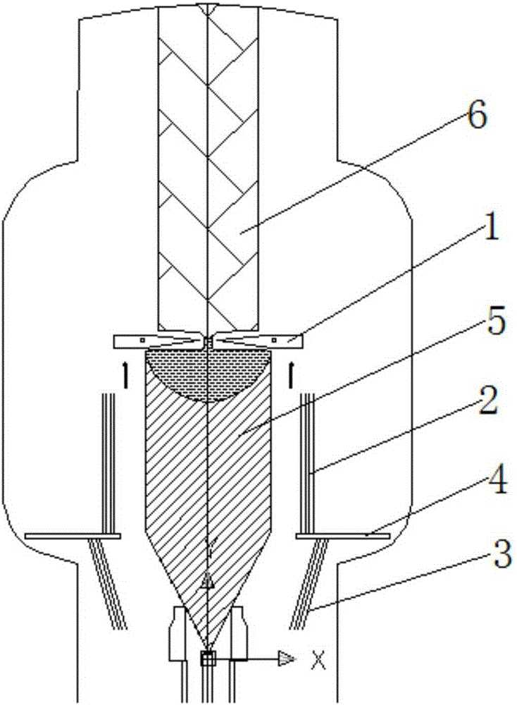
[0028] Such as Figure 1-4 As shown, a heat field structure for melting 8-12 inch silicon single crystal 5 in the drawing zone, including a sharp-angle coil 1, a middle heat shield 2 and a lower heat shield 3;

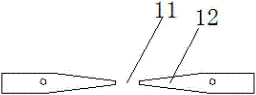
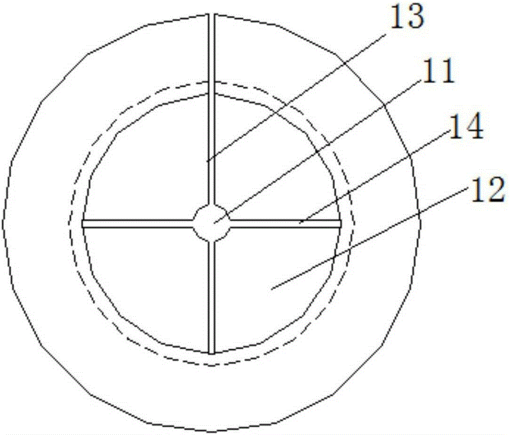
[0029] The pointed coil 1 is located in the melting zone between the polycrystalline rod 6 and the single crystal rod 5 in the furnace, the polycrystalline rod 6 is located in the upper part of the furnace, and the single crystal rod 5 is located in the polycrystalline rod 5 Below the crystal bar material, the pointed coil 1 is a circular coil, the diameter of the circular coil is 160-300mm, and the center of the circular coil is provided with a coil eye 11. Between the edge an...


PUM


Abstract

The invention provides a thermal field structure for drawing a zone-melting 8-12-inch silicon single crystal. The thermal field structure comprises a sharp-angled coil, a middle thermal shield and a lower thermal shield, wherein the sharp-angled coil is located at a melting zone between a polycrystal rod and a single-crystal rod in a furnace body; the sharp-angled coil is a round coil; a coil eye is formed in the center of the round coil; a plurality of coil seams which are in circumferential distribution by taking the center of the round coil as a starting point are arranged between the outer edge of the round coil and the coil eye; the coil between every two adjacent coil seams forms a sharp-angled step; a ring-shaped steel plate is arranged in the furnace body; the middle thermal shield is fixed to the upper end of the ring-shaped steel plate; the lower thermal shield is fixed to the lower end of the steel plate. According to the thermal field structure for drawing the zone-melting 8-12-inch silicon single crystal, owing to arrangement of the sharp-angled coil, the raw material melting capability of the coil can be enhanced, the power of the coil can be reduced, and poor crystal pulling waist forms caused by high power are avoided or reduced; owing to arrangement of the middle thermal shield and the lower thermal shield, the probability of dislocation is lowered.

Description

technical field [0001] The invention belongs to the field of single crystal silicon production equipment, and in particular relates to a thermal field structure for melting 8-12 inch silicon single crystal in a drawing zone. Background technique [0002] The growth of monocrystalline silicon by zone melting is currently the most advanced application technology for the production of single crystal silicon, so it is used in high-end power electronic devices. With the development of power electronic devices, large diameters have become an inevitable trend. The increase of the single crystal diameter may lead to the following problems: Firstly, the diameter of the raw material increases, and the power of the required generator increases accordingly, which leads to an increase in the probability of ionization breakdown, and an increase in the probability of uneven feeding or puncture of the feeding material ; Secondly, the increase of thermal stress leads to an increase in the pr...

Claims


Application Information

Patent Timeline
IPC IPC(8): C30B13/16C30B29/06
Inventor 娄中士刘琨石海涛杨旭洲郝大维刘铮张雪囡由佰玲王彦君
Owner TIANJIN ZHONGHUAN ADVANCED MATERIAL TECH
Why Eureka
Try Eureka