Optical close range correction, photo mask production and graphic method

A technology of optical close-up and manufacturing method, which is applied in the direction of optics, photo-engraving process of pattern surface, originals for opto-mechanical processing, etc. Inconsistent density and other problems, to achieve the effect of improving image quality

Inactive Publication Date: 2009-06-17
SEMICON MFG INT (SHANGHAI) CORP
View PDF1 Cites 4 Cited by
  • Summary
  • Abstract
  • Description
  • Claims
  • Application Information

AI Technical Summary

Problems solved by technology

[0006] In the prior art, since the auxiliary graphics corresponding to the auxiliary graphics of the mask should not be formed on the photoresist layer of the wafer, the size of the auxiliary layout graphics should be smaller than the layout circuit graphics, so that the layout circuit graphics in the semi-dense area of ​​the device and the isolated area of ​​​​the device The density of the layout pattern composed of the layout auxiliary pattern and the layout circuit pattern density of the device-dense area is inconsistent, resulting in the difference between the circuit pattern of the semi-dense area of ​​the device and the isolated area of ​​the device and the circuit pattern of the device-dense area after transfer to the wafer. The critical dimensions are quite different, such as figure 2 As shown, when the same light intensity threshold (shown by the dotted line) is used to transfer the layout circuit pattern of the device isolated area and the device dense area to the wafer, the criticality of the circuit pattern of the device isolated area and the circuit pattern of the device dense area The difference in size is greater than 0.03 μm, which in turn affects the imaging quality of semiconductor devices

Method used


Image

  • Optical close range correction, photo mask production and graphic method
  • Optical close range correction, photo mask production and graphic method
  • Optical close range correction, photo mask production and graphic method

Examples


Embodiment Construction

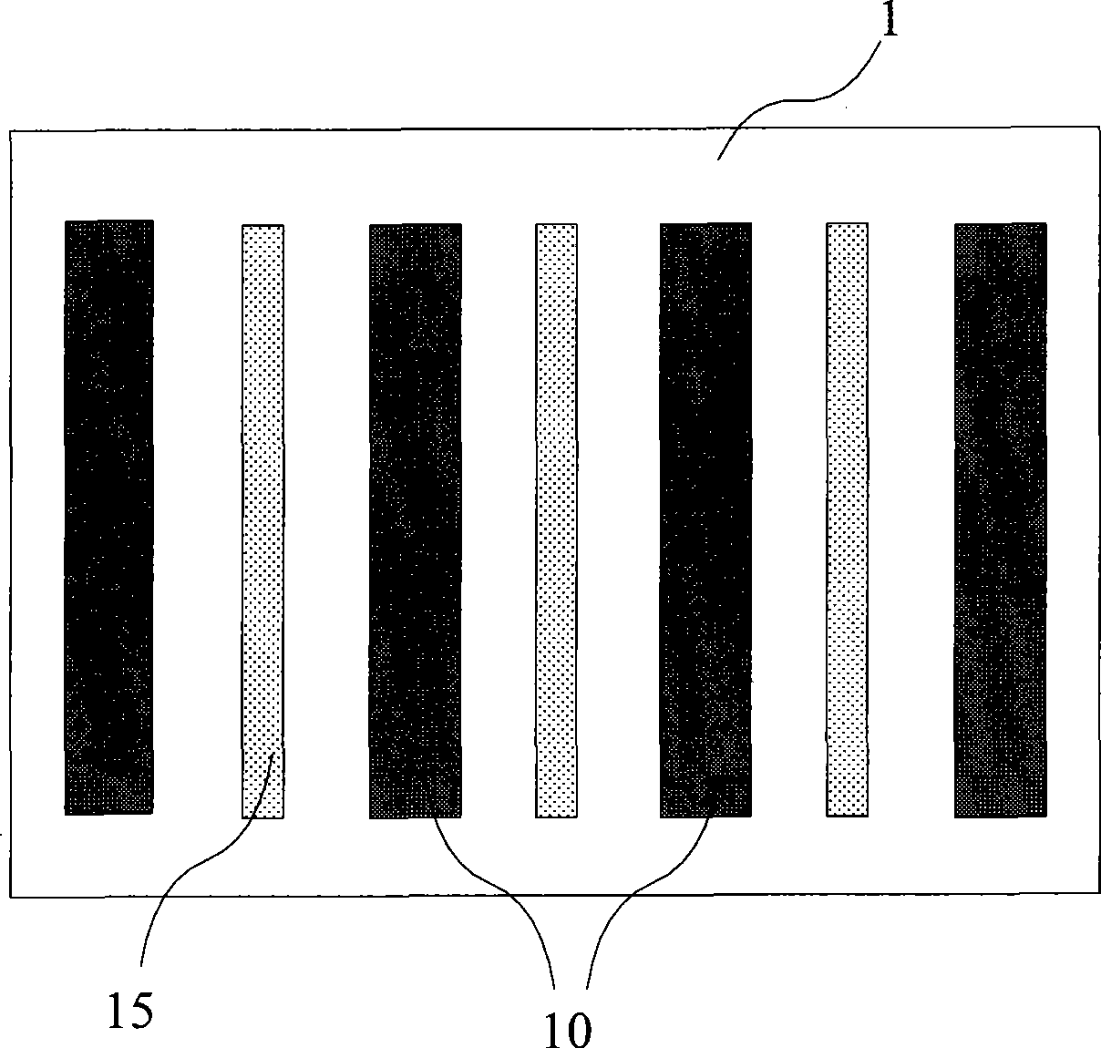
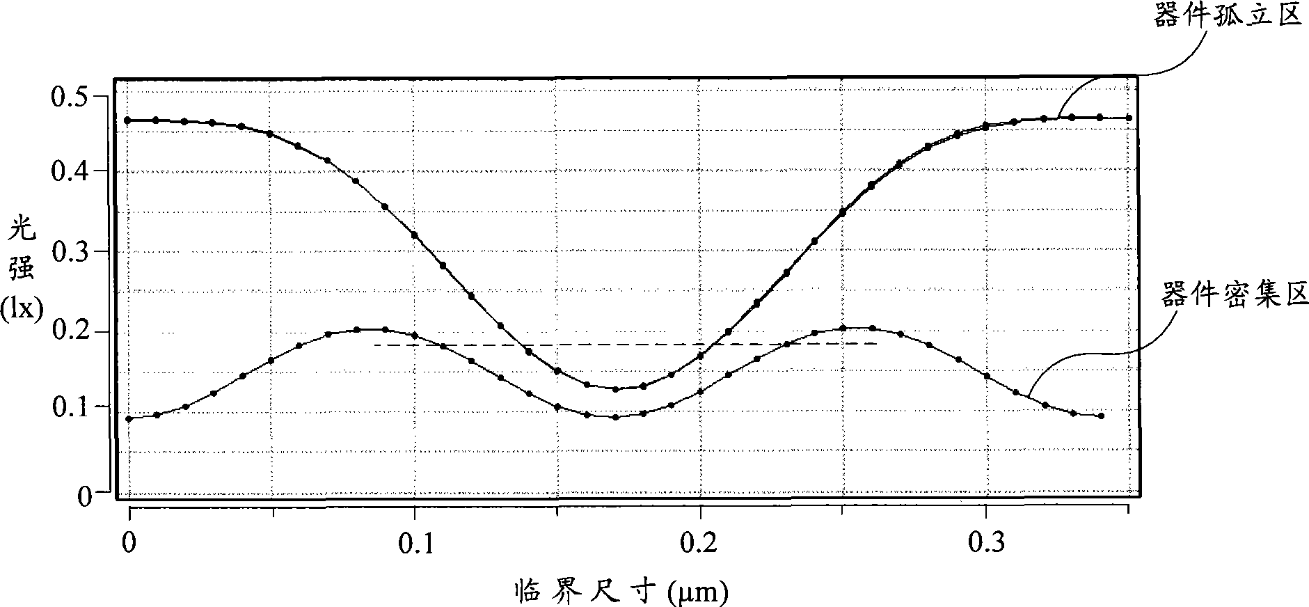
[0033] According to the density of semiconductor devices on the wafer, it can be divided into device-dense area, device semi-dense area and device isolated area. The distance between circuit patterns in the device-dense area is equal to 1CD, and the distance between circuit patterns in the device semi-dense area is greater than 1CD and less than Equal to 3CD, the distance between the circuit patterns in the isolated area of ​​the device is greater than 3CD.

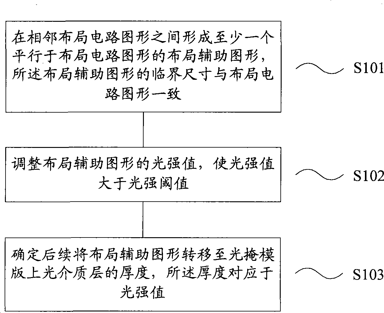
[0034] Forming the circuit pattern on the photoresist layer of the wafer is to use the photomask plate manufacturing equipment to transfer the designed layout circuit pattern to the photomask plate, and then use the exposure device to transfer the reticle circuit pattern on the photomask plate onto the photoresist layer of the wafer. Therefore, adding layout auxiliary patterns around the layout circuit patterns can reduce the CD variation of the circuit patterns formed on the photoresist layer of the wafer.

[0035]In th...


PUM


Abstract

An optical short-distance correcting method comprises: at least one layout auxiliary pattern which is parallel to layout circuit patterns is formed between the adjacent layout circuit patterns, wherein, the critical dimension of the layout auxiliary pattern is consistent with that of the layout circuit patterns; a light intensity value of the layout auxiliary pattern is adjusted, so that the light intensity value is larger than a light intensity threshold value; and the thickness of an optical medium layer for transferring the layout auxiliary pattern to a photomask plate subsequently is determined, wherein, the thickness corresponds to the light intensity value. The invention also provides a manufacturing method of the photomask plate and a graphical method thereof. The invention causes the critical dimensions of circuit patterns of a device semi-concentration area and a device isolation area are consistent with the critical dimensions of the circuit patterns of a device concentration area, and the layout auxiliary pattern does not form an image on a wafer.

Description

technical field [0001] The invention relates to the technical field of semiconductor manufacturing, in particular to optical short-distance correction, photomask production and patterning methods. Background technique [0002] With the rapid development of semiconductor manufacturing technology, in order to achieve faster computing speed, larger data storage capacity and more functions of semiconductor devices, semiconductor chips are developing towards higher integration. The higher the integration degree of the semiconductor chip, the smaller the critical dimension (CD, Critical Dimension) of the semiconductor device. [0003] However, due to the impact of the resolution limit of the exposure tool (optical exposure tool), the optical proximity effect is likely to occur when exposing these highly densely arranged reticle circuit patterns to the wafer. (OPE, optical proximity effect), such as right-angled corner rounded (right-angled corner rounded), line end shortened (lin...

Claims


Application Information

Patent Timeline
Patent Type & Authority Applications(China)
IPC IPC(8): G03F1/14G03F1/00G03F1/36
Inventor 张飞
Owner SEMICON MFG INT (SHANGHAI) CORP
Why Eureka
Try Eureka