Production method for floating gate of flash memory in grating

A manufacturing method and floating gate technology, applied in semiconductor/solid-state device manufacturing, electrical components, semiconductor devices, etc., can solve problems such as unfavorable process reliability, incomplete erasure efficiency, and difficulty in cutting-edge optimization, so as to reduce erasure Effects of invalidation, optimization of fluctuations, and reduction of intra-chip discontinuities

Inactive Publication Date: 2009-06-17
SHANGHAI HUA HONG NEC ELECTRONICS
View PDF0 Cites 1 Cited by
  • Summary
  • Abstract
  • Description
  • Claims
  • Application Information

AI Technical Summary

Problems solved by technology

[0002] In the prior art, for split-gate flash memory, the tip of the floating gate is usually formed by local field oxidation, but in this method, there are many steps that affect the shape of the tip, the production efficiency is low, and it is not easy to damage the tip. Moreover, the structure formed by the local oxidation method has a large gap between the middle and the periphery of the flash memory array, which is not conducive to the reliability of the process
From the perspective of erasing efficiency, when performing erasing operations on flash memory, the efficiency is easily affected by the shape of the tip, resulting in incomplete erasing

Method used


Image

  • Production method for floating gate of flash memory in grating
  • Production method for floating gate of flash memory in grating
  • Production method for floating gate of flash memory in grating

Examples


Embodiment Construction

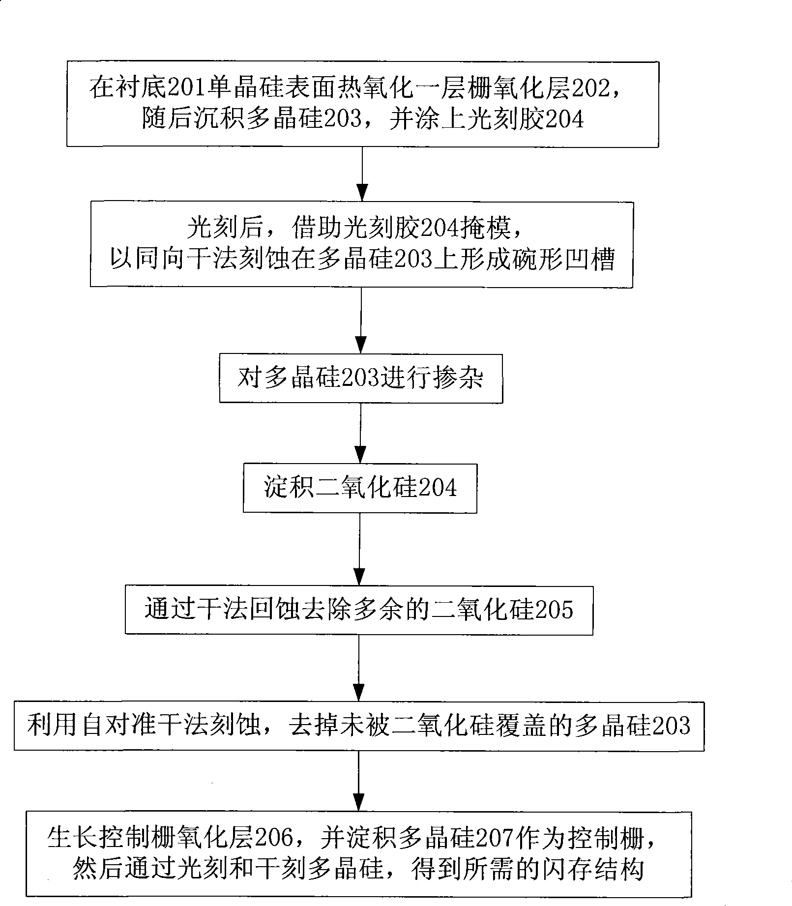
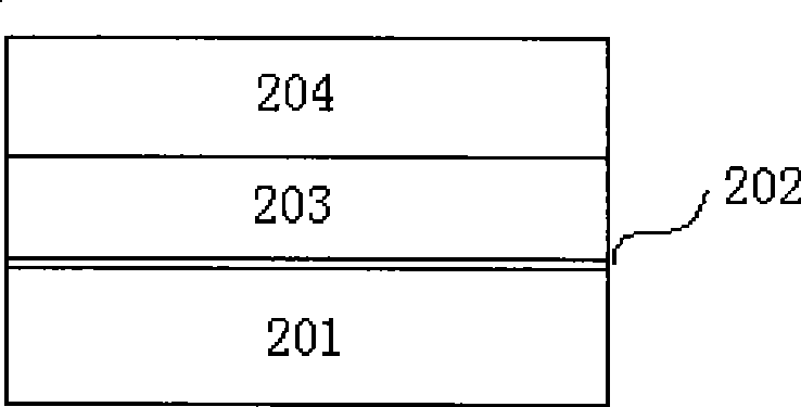
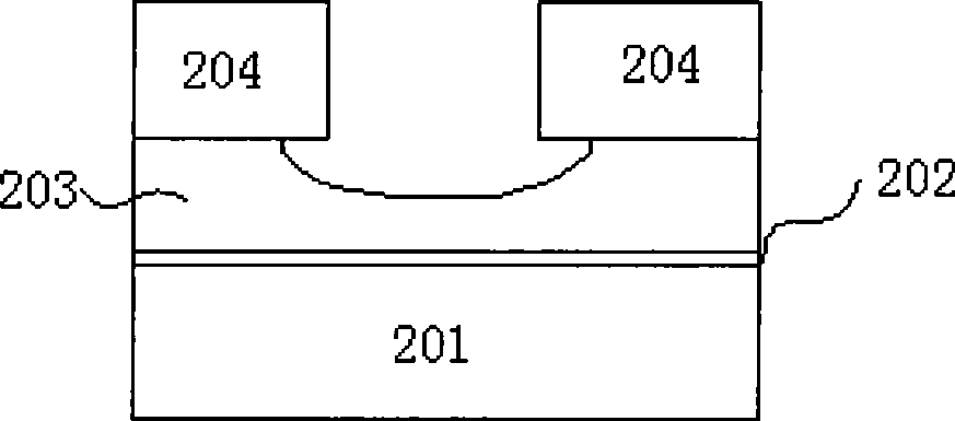
[0015] In one embodiment, such as figure 1 and Figures 2a-2g As shown, the method for manufacturing the floating gate of the split-gate flash memory of the present invention includes the following steps:

[0016] (1) Split-gate flash memory has a structure different from ordinary flash memory. In order to ensure that hot electrons can be written more effectively in split-gate flash memory, the P-type well and source-drain of split-gate flash memory are completed on the silicon substrate 201. After ion implantation and other processes, it is necessary to thermally oxidize a layer on the surface of the silicon substrate 201 with a thickness of 75-105 The thin film 202 in the range is used as the gate oxide layer 202 of the floating gate, and then a layer with a thickness of 3500-4500 is deposited on the gate oxide layer 202 range of polysilicon 203, and then coated with a layer thickness of about 10,000 photoresist 204 to carry out photoetching to the polysilicon 203, at ...


PUM


Abstract

The invention discloses a manufacturing method for floating gates of split-gate flash memories, which comprises steps of firstly using photoresist as a mask and utilizing isotropic dry etching to form a bowl-shaped groove of a floating gate, secondarily, depositing a silicon dioxide layer and utilizing the dry etch-back technique to form a semicircular oxide layer, and finally, utilizing self-aligned dry etching to etch away polysilicon outside an oxide region, thereby obtaining sharp periphery of the floating gate, guaranteeing the shape of the finally formed floating gate be unaffected by other operating steps during the manufacturing process of split-gate flash memories, reducing step on chip in flash memory arrays of the split-gate flash memory, increasing production efficiency and further simplifying optimization for pointed ends of the floating gate with small fluctuation, besides, the manufacturing method is simple to realize and reduces manufacturing cost to some extent. The manufacturing method further can guarantee reducing erase failure and erase voltage when the flash memory executes erasing actions, and thereby the flash memory unit is easier to control.

Description

technical field [0001] The invention relates to the field of manufacturing split-gate flash memory, in particular to a method for manufacturing the floating gate of split-gate flash memory. Background technique [0002] In the prior art, for split-gate flash memory, the tip of the floating gate is usually formed by local field oxidation, but in this method, there are many steps that affect the shape of the tip, the production efficiency is low, and it is not easy to damage the tip. In addition, the structure formed by the local oxidation method has large gaps in the middle and periphery of the flash memory array, which is not conducive to the reliability of the process. From the perspective of erasing efficiency, when performing erasing operations on flash memory, the efficiency is easily affected by the shape of the tip, resulting in incomplete erasing. Contents of the invention [0003] The technical problem to be solved by the present invention is to provide a floating...

Claims


Application Information

Patent Timeline
Patent Type & Authority Applications(China)
IPC IPC(8): H01L21/28H01L21/336
Inventor 贾晓宇金勤海
Owner SHANGHAI HUA HONG NEC ELECTRONICS
Why Eureka
Try Eureka