Method for manufacturing flash memory floating gate

A manufacturing method and floating gate technology, applied in the field of flash memory manufacturing, can solve the problems of difficult cutting-edge optimization, low production efficiency, incomplete erasing, etc., and achieve the effects of reducing erasure failure, improving production efficiency, and being easy to control.

Active Publication Date: 2009-04-22
SHANGHAI HUAHONG GRACE SEMICON MFG CORP
View PDF0 Cites 0 Cited by
  • Summary
  • Abstract
  • Description
  • Claims
  • Application Information

AI Technical Summary

Problems solved by technology

In the manufacturing process of the existing floating gate structure flash memory, the tip of the floating gate is usually formed by the local field oxidation method. This method has many subsequent steps that affect the shape of the tip, so it will lead to low production efficiency and is not easy to damage the tip. Optimized, and when the flash memory is erased, the efficiency is easily affected and the erase is incomplete

Method used


Image

  • Method for manufacturing flash memory floating gate
  • Method for manufacturing flash memory floating gate
  • Method for manufacturing flash memory floating gate

Examples


Embodiment Construction

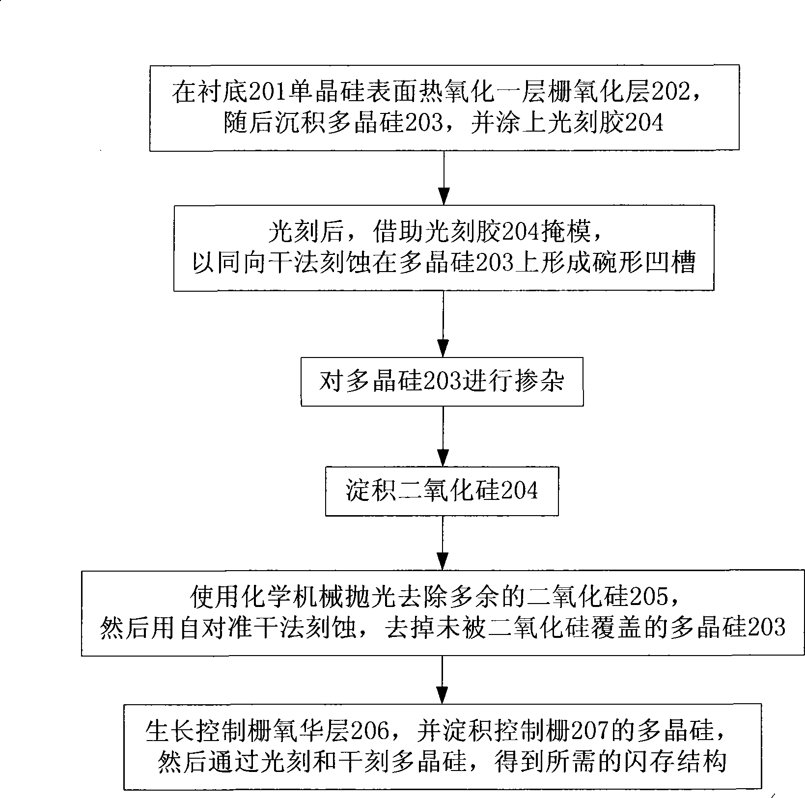
[0014] pass below figure 1 and Fig. 2, the flash memory floating gate manufacturing method of the present invention is described in detail, the method mainly includes the following steps:

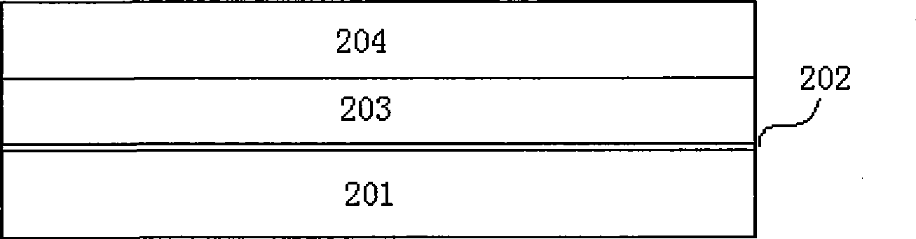
[0015] (1) The thickness of a layer of thermal oxidation on the surface of substrate 201 single crystal silicon is The thin film 202 within the range is used as the gate oxide layer 202 of the floating gate, and then a layer with a thickness of polysilicon 203 within the range, and then coated with photoresist 204 to perform photoetching on the polysilicon 203, specifically as Figure 2a shown.

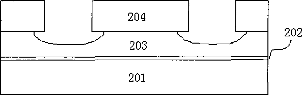
[0016] (2) Utilize known photolithography technology to carry out photoetching to described polysilicon 203, then with the aid of photoresist 204 mask, form the bowl-shaped groove of floating gate on described polysilicon 203 with dry etching (that is flash memory cell area), specifically as Figure 2b shown.

[0017] (3) if Figure 2c As shown, the polysilicon 203 is doped with phosphorus ...


PUM


Abstract

The invention discloses a method for manufacturing a flash floating gate, a bowl-shaped groove of the floating gate is formed by isotropic dry etching with the help of a photoresist mask; then silicon dioxide is deposited in the bowl-shaped groove, the silicon dioxide which is positioned at the outside of the bowl-shaped groove is removed by using the chemical polishing method, thereby forming the floating gate; and then polycrystalline silicon which is positioned out of a flash unit is removed by the self-alignment mode with the help of the dry etching to form the acute periphery of the floating gate, thereby ensuring the floating gate structure not to be affected by other operations during the manufacturing process of the flash, further improving the production efficiency and leading the process to be easy in the optimization of the tip of the floating gate and have smaller fluctuations. The method can reduce the erase failure and reduce the erase voltage in the implementation of the erase action of the flash, thereby leading the flash unit to be easier to control.

Description

technical field [0001] The invention relates to the field of flash memory manufacturing, in particular to a method for manufacturing a flash memory floating gate. Background technique [0002] A flash memory with a floating gate structure usually uses polysilicon with a tip as a floating gate, and the tip of the floating gate is covered by a control gate. When erasing the flash memory, by connecting the source and drain to a low voltage and the control gate to a high voltage, the electrons in the floating gate will tunnel through the gap between the floating gate and the control gate due to the high electric field near the tip of the floating gate. The oxide layer flows to the control gate. In the manufacturing process of the existing floating gate structure flash memory, the tip of the floating gate is usually formed by the local field oxidation method. This method has many subsequent steps that affect the shape of the tip, so it will lead to low production efficiency and ...

Claims


Application Information

Patent Timeline
Patent Type & Authority Applications(China)
IPC IPC(8): H01L21/28H01L21/8247H01L27/11521
Inventor 贾晓宇金勤海
Owner SHANGHAI HUAHONG GRACE SEMICON MFG CORP
Why Eureka
Try Eureka