Active-matrix addressing liquid-crystal display device using lateral electric field and having two storage capacitors

a technology of active matrix and lateral electric field, which is applied in the direction of identification means, instruments, optics, etc., can solve the problems of low aperture ratio, reduced transmittance, and high probability of delay of corresponding gate line signal, and achieve higher transmittance and fabrication yield

Inactive Publication Date: 2005-03-01
NEC LCD TECH CORP
View PDF9 Cites 37 Cited by
  • Summary
  • Abstract
  • Description
  • Claims
  • Application Information

AI Technical Summary

Benefits of technology

Accordingly, an object of the present invention is to provide an active-matrix addressing LCD device using lateral electric field that realizes a higher transmittance and a higher fabrication yield.
Therefore, the penetrating light is blocked by the interconnection electrodes. However, the electrodes are sufficiently apart from the liquid crystal layer. Thus, the interconnection electrodes will apply very weak electric field to the liquid crystal in the liquid crystal layer. This means that electric field fluctuation for the respective columns in each pixel will be small. In other words, the interconnection electrodes do not affect badly the obtainable transmittance, which corresponds to the device of the first embodiment where the interconnection electrodes are formed by the transparent pixel electrodes. As a result, the device of the second aspect of the invention has the same advantages as those of the device of the first aspect of the invention.

Problems solved by technology

On the other hand, the IPS mode LCD device has a disadvantage that an obtainable aperture ratio is low and as a result, the transmittance is reduced.
In this method, the storage capacitor between the prior-stage scanning line and the corresponding pixel electrode serves as a load of the corresponding scanning line signal and therefore, there are disadvantages that the corresponding gate line signal is likely to be delayed and that the panel transmittance within the panel plane is likely to be dispersed.
This makes it likely to delay the transmission of the data line signals.
As a result, the storage capacitor with a sufficiently large capacitance for stable displaying operation is unable to be formed between the level of the data lines and the level of the common electrode.
However, the probability that the fabrication yield degrades due to the electrical short circuit between the lines will increase and at the same time, the switching characteristics of the TFTs will be badly affected.
Furthermore, with the IPS mode LCD device, as shown in FIG. 22, the direction of the electric field applied to the liquid crystal layer is complicated at the end of each “column”.
As a result, the abnormal domain scarcely makes contribution to increase of the panel transmittance of the LCD device, which means that the panel transmittance is lowered.
If the pixel potential layers are formed in each pixel, which are used to form two or more storage capacitors in each pixel, are constituted in such a way as to be electrically connected to each other by way of parts of a conductive layer, it was found that the following problems occurred.
The first problem is that the total panel transmittance is lowered.
The second problem is that the effective aperture ratio is decreased and the transmittance is lowered.
The third problem is that the luminance is lowered in the all-white displaying operation.
Thus, the electric field fluctuates in each pixel, which results in the luminance lowering in the all-white displaying operation.
The fourth problem is that the fabrication yield is lowered.
Specifically, the transparent pixel electrodes and the transparent common electrode tend to be disconnected locally due to the step-shaped gaps between the pixel and common electrodes and their underlying metal layers (i.e., the scanning lines and the data lines) in the etching process, resulting in undesired disconnections in the patterned electrodes.
Thus, the lateral electric field is not applied partially to the liquid crystal layer, resulting in a defect in the displaying operation.
This leads to lowering in the fabrication yield of the LCD device.

Method used


Image

  • Active-matrix addressing liquid-crystal display device using lateral electric field and having two storage capacitors
  • Active-matrix addressing liquid-crystal display device using lateral electric field and having two storage capacitors
  • Active-matrix addressing liquid-crystal display device using lateral electric field and having two storage capacitors

Examples


first embodiment

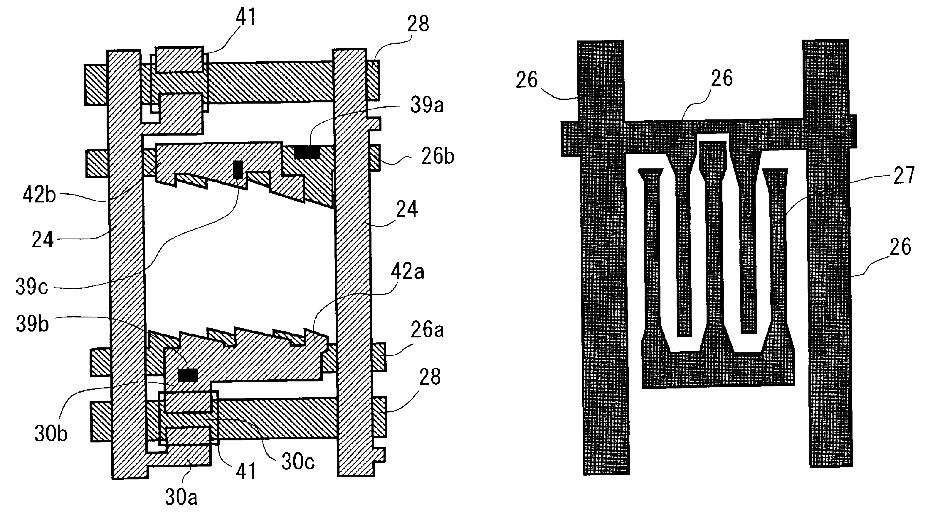
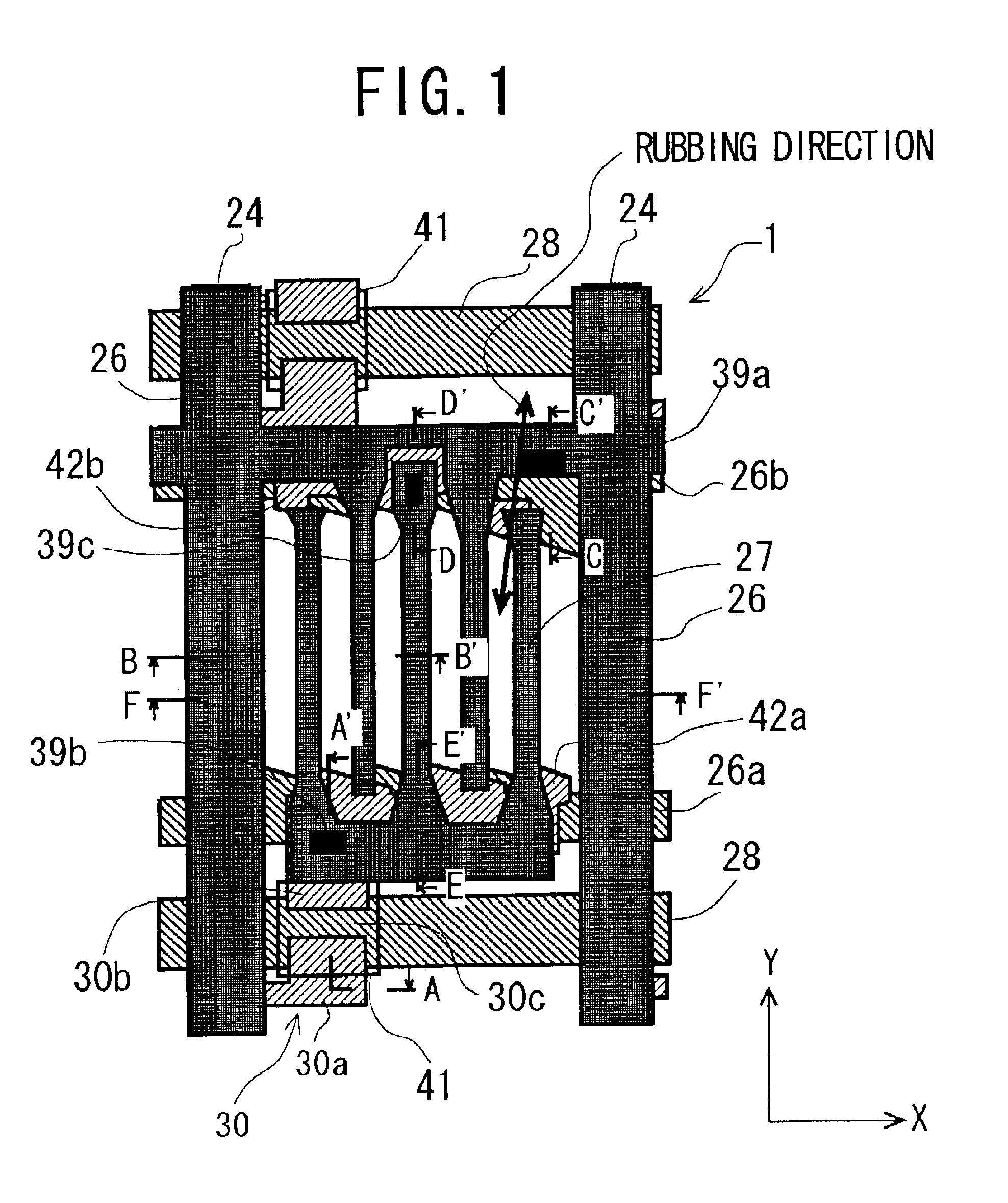
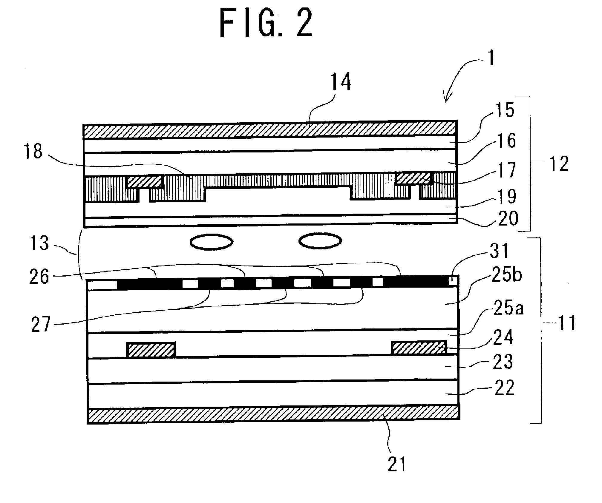
An IPS mode active-matrix addressing LCD device 1 according to a first embodiment of the invention has the structure as shown in FIGS. 1, 2, 3A, 3B and 4.

As clearly seen from FIG. 2, the LCD device 1 according to the first embodiment comprises a rectangular active element substrate 11, a rectangular opposite substrate 12 coupled with the substrate 11 parallel to each other, and a liquid crystal layer 13 sandwiched by the substrates 11 and 12 and confined in the gap between the substrates 11 and 12. The combination of the two substrates 11 and 12 and the intervening liquid crystal layer 13 is referred as the “LCD panel” later.

In this specification, the side or surface of the active element substrate 11 near the liquid crystal layer 13 is termed the “inner side” or “inner surface” and the other side thereof far from the liquid crystal layer 13 is termed the “outer side” or “outer surface”. This definition is applied to the opposite substrate 12 as well.

As shown in FIG. 2, the active e...

second embodiment

FIGS. 7 and 8 and FIGS. 9A and 9B show an IPS mode active-matrix addressing LCD device 2 according to a second embodiment of the invention.

FIG. 7 shows a plan view of the active element substrate. FIG. 8 shows the cross-sectional view along the line F-F′ in FIG. 7. FIGS. 9A and 9B show the layout of the patterns of the layers lower than the data lines, and the layout of the layer of the data lines, respectively. In these figures, the same reference numerals or symbols are attached to the same elements as shown in the LCD device 1 according to the above-described first embodiment. Thus, the explanation about the same elements is omitted here for the sake of simplification of description.

Comparing the LCD device 2 of the second embodiment with that of the first embodiment, the configuration of the second embodiment is the same as that of the first embodiment with respect to the active element substrate 11, except for the structure to electrically interconnect the pixel potential layer...

third embodiment

FIGS. 11 and 12 and FIGS. 13A and 13B show an IPS mode active-matrix addressing LCD device 3 according to a third embodiment of the invention.

FIG. 11 shows a plan view of the active element substrate. FIG. 12 shows the cross-sectional view along the line F-F′ in FIG. 11. FIGS. 13A and 13B show the layout of the patterns of the layers lower than the data lines, and the layout of the layer of the data lines, respectively. In these figures, the same reference numerals or symbols are attached to the same elements as shown in the LCD device 1 according to the above-described first embodiment. Thus, the explanation about the same elements is omitted here for the sake of simplification of description.

Comparing the LCD device 3 of the third embodiment with that of the second embodiment, the configuration of the third embodiment is the same as that of the second embodiment with respect to the active element substrate 11, except for the structure to electrically interconnect the pixel potenti...


PUM

PropertyMeasurementUnit
dielectricaaaaaaaaaa
coloraaaaaaaaaa
transparentaaaaaaaaaa

Abstract

An active-matrix addressing LCD device using lateral electric field realizes a higher transmittance and a higher fabrication yield and improves the aperture ratio without raising the fabrication cost. A first one of the common electrode lines, a first one of the pixel potential layers, and an intervening dielectric layer constitute a first storage capacitor for each of the pixels and at the same time, a second one of the common electrode lines, a second one of the pixel potential layers, and the intervening dielectric layer constitute a second storage capacitor for the same pixel. The first and second pixel potential layers are electrically connected to each other by way of a corresponding transparent pixel electrode. Therefore, the rotation of the liquid crystal molecules caused by applied electric field makes full contribution to the panel transmittance, preventing the obtainable total panel transmittance from lowering. This means that a higher transmittance is obtainable. An interconnection electrode may be additionally provided for the same purpose.

Description

BACKGROUND OF B THE INVENTION1. Field of the InventionThe present invention relates generally to a Liquid-Crystal Display (LCD) device. More particularly, the invention relates to an active-matrix addressing LCD device using lateral electric field, which improves the transmittance and the fabrication yield.2. Description of the Related ArtActive-matrix addressing LCD devices that use Thin-Film Transistors (TFTs) as the switching elements for respective pixels, which provide high-level image quality, have been extensively used as display devices for portable or note-book type computers. Recently, they have been used as monitoring devices of space-saving desktop computers as well.Active-matrix addressing LCD devices are classified into two types. With the devices of the first type, the orientation of the molecular axis of liquid crystal, which is called the “director”, is rotated in a plane perpendicular to the pair of substrates, thereby displaying desired images. With the devices of...

Claims


Application Information

Patent Timeline
Patent Type & Authority Patents(United States)
IPC IPC(8): G02F1/13G02F1/1362G02F1/1343G02F1/1368G09F9/30G09F9/35H01L21/336H01L29/786
CPCG02F1/136213G02F1/134363G02F1/1343
Inventor MATSUMOTO, KIMIKAZUHANNUKI, TAKAHISA
Owner NEC LCD TECH CORP
Why Eureka
Try Eureka