Three-dimensional stack chip structure with vertical electrical self-connection and manufacturing method thereof

A chip structure and manufacturing method technology, applied in semiconductor/solid-state device manufacturing, circuits, electrical components, etc., can solve problems such as high cost, complex process and time-consuming, and achieve low-cost effects

Inactive Publication Date: 2009-06-24
IND TECH RES INST
View PDF14 Cites 16 Cited by
  • Summary
  • Abstract
  • Description
  • Claims
  • Application Information

AI Technical Summary

Problems solved by technology

[0004] The above-mentioned known three-dimensional stacking chip manufacturing methods all need to use quite expensive equipment and the process is complicated and time-consuming, making these three-dimensional stacking chip manufacturing methods cost a relatively high cost

Method used


Image

  • Three-dimensional stack chip structure with vertical electrical self-connection and manufacturing method thereof
  • Three-dimensional stack chip structure with vertical electrical self-connection and manufacturing method thereof
  • Three-dimensional stack chip structure with vertical electrical self-connection and manufacturing method thereof

Examples


Embodiment Construction

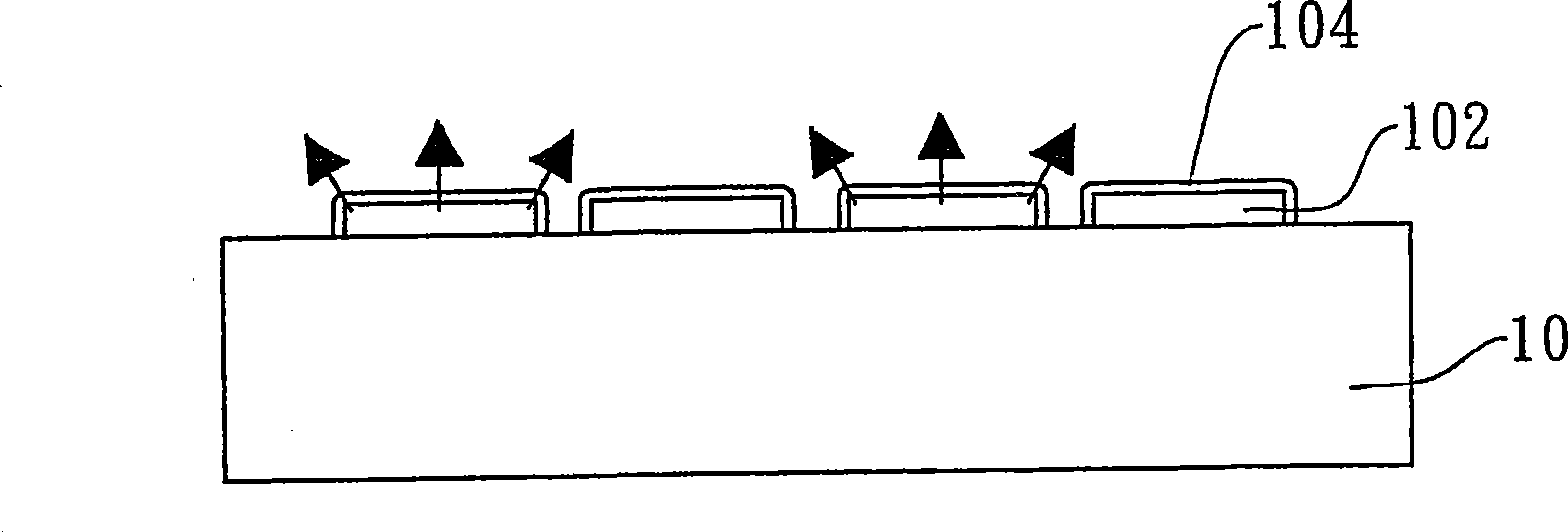
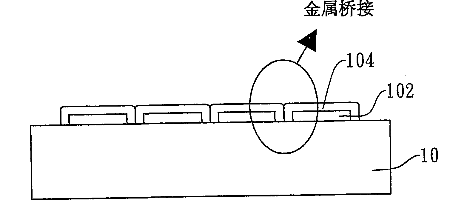
[0044] Figure 1A and Figure 1B It is a schematic diagram of the technology for forming electrical self-connection between metal pads 102 on a chip 10, which adopts an electroless plating process (electroless plating process) to deposit metal 104 on each metal pad 102, so that the deposited metal 104 grows isotropically, Furthermore, a metal bridge is formed between each metal pad 102 to form an electrical self-connection between each metal pad 102 . The present invention further applies this concept to the structure of three-dimensional stacked chips, and establishes vertical electrical conduction between three-dimensional stacked chips by a simple electroless plating process.

[0045] The three-dimensional stacked chip structure with vertical electrical self-connection of the present invention and its manufacturing method will be described in detail as follows through the following embodiments with accompanying drawings:

[0046] Figure 2A to Figure 2J It is a structura...


PUM


Abstract

The invention provides a vertically and electrically self-connected three-dimensional stack chip structure and a manufacturing method thereof; wherein, respective electrical conductive wire layers are formed among the three-dimensional stack chips and then extended to the sidewalls of the chips; the respective electrical conductive wire layers which are buried among the layers and exposed out of the sidewalls of the chips are used to carry out electroless metal self-deposition to grow up isotropically, so as to form a vertical and electrical conductive wire along the sidewalls of the stack chips; the vertical and electrical conductive wire is then connected with each electrical conductive layer to complete the vertical and electrical self-connection of the three-dimensional stack chips.

Description

technical field [0001] The present invention relates to a three-dimensional stacked chip structure and its manufacturing method; in particular, it relates to a three-dimensional stacked chip structure with vertical electrical self-connection and its manufacturing method. Background technique [0002] In order to meet the demand trend of thin, light, small, power-saving and high-performance electronic products in the future, the current traditional semiconductor two-dimensional (2D) chip structure and circuit connection methods no longer meet future product needs. Therefore, changing the two-dimensional chip wire layout method to a three-dimensional (3D) connection method can effectively solve the technical bottleneck encountered by the traditional two-dimensional chip wire layout method. The stacking method of three-dimensional chips can effectively increase the component density per unit area, reduce chip size and energy loss, and other advantages. [0003] U.S. Patent No....

Claims


Application Information

Patent Timeline
Patent Type & Authority Applications(China)
IPC IPC(8): H01L25/00H01L25/065H01L23/48H01L21/60
CPCH01L24/82H01L2224/13
Inventor 张恕铭
Owner IND TECH RES INST
Why Eureka
Try Eureka