Semiconductor light emitting element and method for fabricating the same

A light-emitting element and semiconductor technology, which is applied in the direction of semiconductor devices, semiconductor lasers, electrical components, etc., can solve the problems of reducing production efficiency and reducing the number of semiconductor light-emitting elements, so as to improve production efficiency, prevent leakage current, and suppress the deterioration of electrical characteristics Effect

Inactive Publication Date: 2009-07-01
PANASONIC CORP
View PDF1 Cites 11 Cited by
  • Summary
  • Abstract
  • Description
  • Claims
  • Application Information

AI Technical Summary

Problems solved by technology

[0004] However, in the case of avoiding the core to form the electrode, all the core part becomes useless, and the number of semiconductor light-emitting elements that can be obtained from one wafer decreases, which lowers the production efficiency.

Method used


Image

  • Semiconductor light emitting element and method for fabricating the same
  • Semiconductor light emitting element and method for fabricating the same
  • Semiconductor light emitting element and method for fabricating the same

Examples


no. 1 approach

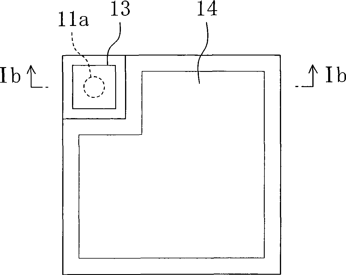
A first embodiment of the present invention will be described with reference to the drawings. Fig. 1 (a) and Fig. 1 (b) show the semiconductor light-emitting element related to the first embodiment of the present invention, Fig. 1 (a) shows the planar structure, Fig. 1 (b) is Ib of Fig. 1 (a) - Ib line profile composition.

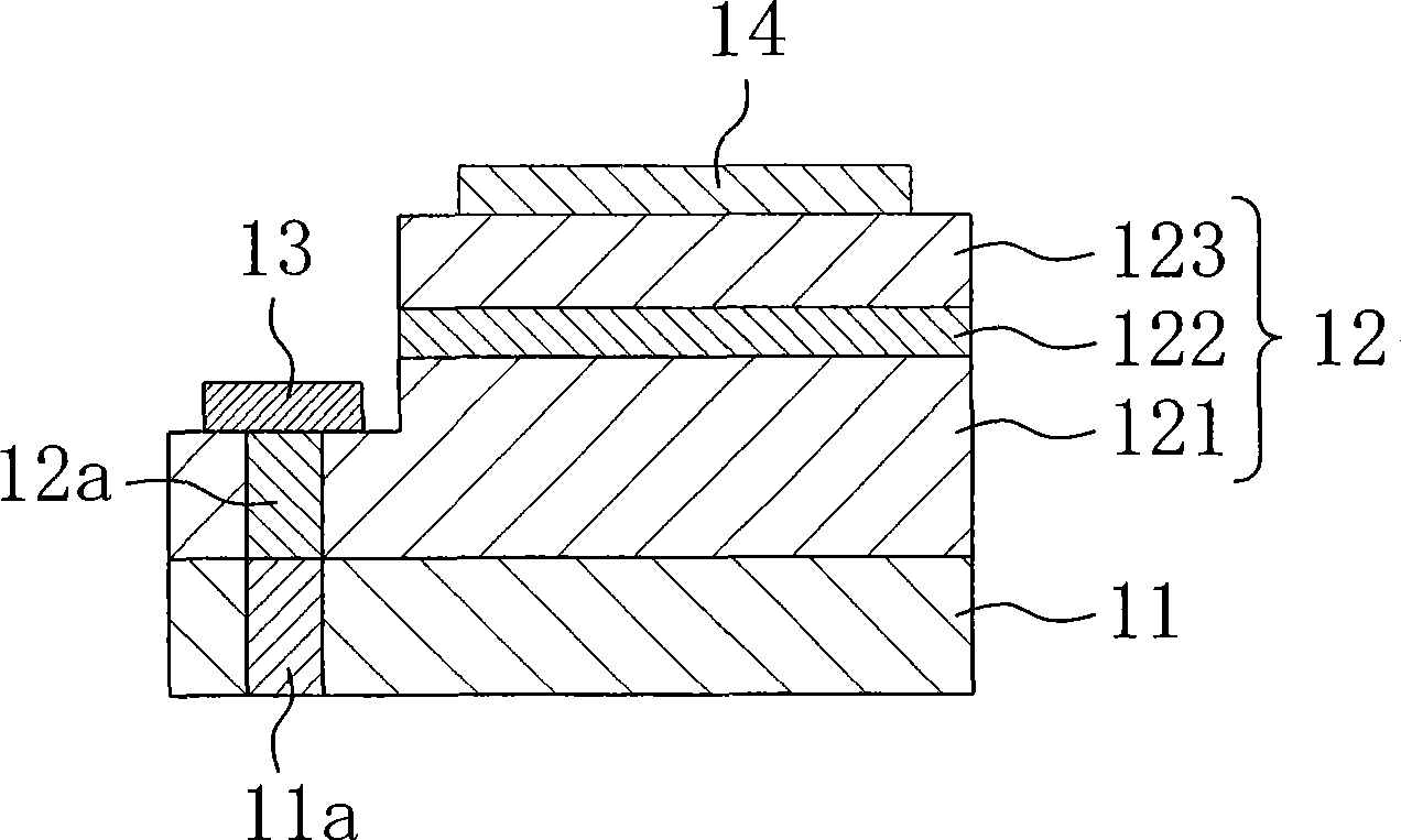
[0018] The semiconductor light emitting element of the first embodiment shown in FIG. 1 is formed on a substrate 11 having a defect concentration region (core) 11a in which crystal defects are concentrated compared with other regions. In this embodiment, the substrate 11 is a single crystal substrate formed of a nitride-based semiconductor such as gallium nitride (GaN), and has a cubic shape with a side length of 1000 μm and a thickness of 300 μm. The core 11a penetrates the substrate 11 from the thickness direction, and is formed at the corner of the substrate in the present embodiment.

[0019] On the substrate 11, a semiconductor layer 12 is formed. T...

no. 2 approach

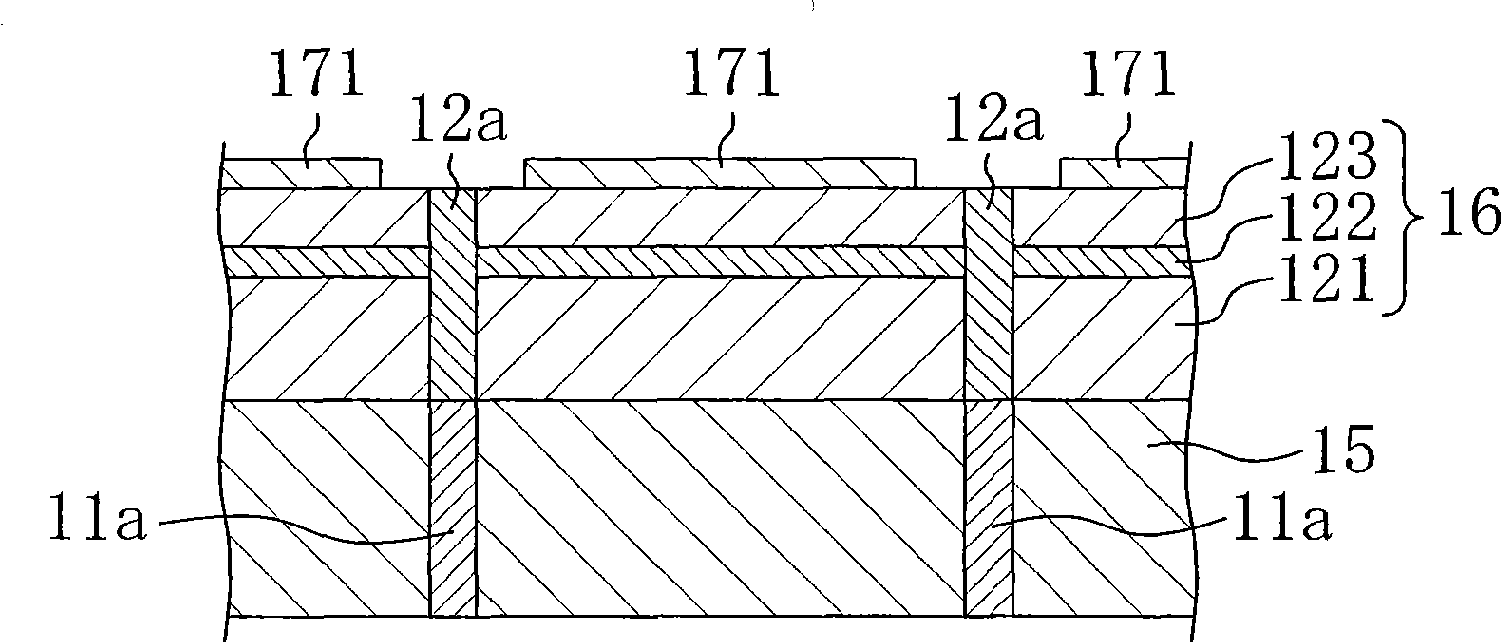
Hereinafter, a second embodiment of the present invention will be described with reference to the drawings. Fig. 6 (a) and Fig. 6 (b) show the semiconductor light-emitting device related to the second embodiment of the present invention, Fig. 6 (a) shows the planar structure, Fig. 6 (b) is VIb of Fig. 6 (a) - Sectional view of line VIb. In FIG. 6, elements having the same configuration as those in FIG. 1 are denoted by the same reference numerals and descriptions thereof are omitted.

[0041] As shown in FIG. 6 , in the semiconductor light emitting element of the present embodiment, the core 11 a is formed almost at the center of the substrate 11 . Thus, the n-side electrode 13 is provided at the center of the semiconductor layer 12 . Thus, the current from p-side electrode 14 flows from the entire p-side electrode 14 to n-side electrode 13 at the center of semiconductor layer 12 through p-type layer 123 , light emitting layer 122 , and n-type layer 121 . Therefore, the curr...


PUM


Abstract

A semiconductor light emitting element includes a substrate 11 having a defect concentrated region 11a which has a crystal defect density higher than in the other region. On the substrate 11, a semiconductor layer 12 is formed. On the defect concentrated region 11a, a first electrode 13 is formed. On the semiconductor layer 12, a second electrode 14 is formed.

Description

technical field [0001] The present invention relates to a semiconductor light emitting element and a manufacturing method thereof, in particular to a semiconductor light emitting element formed on a substrate having a defect-concentrated region with a high crystal defect density and a manufacturing method thereof. Background technique [0002] A semiconductor light-emitting element includes a semiconductor layer formed on a wafer at least with an n-type layer, a light-emitting layer, and a p-type layer. The wafer on which the semiconductor layer is formed preferably has no crystal defects and has good crystallinity. As a method of reducing crystal defects, a method of forming a region called a crystal defect region (core) on a wafer is known. The core (core) is formed to penetrate the wafer, and is a region having a higher density of crystal defects than other regions. By forming a core on a wafer, crystallization defects can be concentrated in the core. By concentrating ...

Claims


Application Information

Patent Timeline
Patent Type & Authority Applications(China)
IPC IPC(8): H01L33/00H01S5/343H01L33/02H01L33/38
CPCH01L33/382H01L33/0062H01L33/025H01L33/12
Inventor 木下嘉将龟井英德
Owner PANASONIC CORP
Why Eureka
Try Eureka