Semiconductor device and cleaning system

A technology for semiconductors and equipment, applied in the field of semiconductor equipment and cleaning systems, can solve the problems of contaminating wafer products, scrapping products, contaminating semiconductor chambers, etc., without reducing the production efficiency of products

Pending Publication Date: 2022-07-26
CHANGXIN MEMORY TECH INC
View PDF6 Cites 1 Cited by
  • Summary
  • Abstract
  • Description
  • Claims
  • Application Information

AI Technical Summary

Problems solved by technology

[0003] The impurities accumulated at the bottom of the machine may rise up with the introduction of process gas during the production process and fall on the wafer undergoing CVD process, thereby contaminating the wafer product and directly leading to product scrap; Impurities on the circle may continue to contaminate other semiconductor chambers as the process continues

Method used


Image

  • Semiconductor device and cleaning system
  • Semiconductor device and cleaning system
  • Semiconductor device and cleaning system

Examples


Embodiment Construction

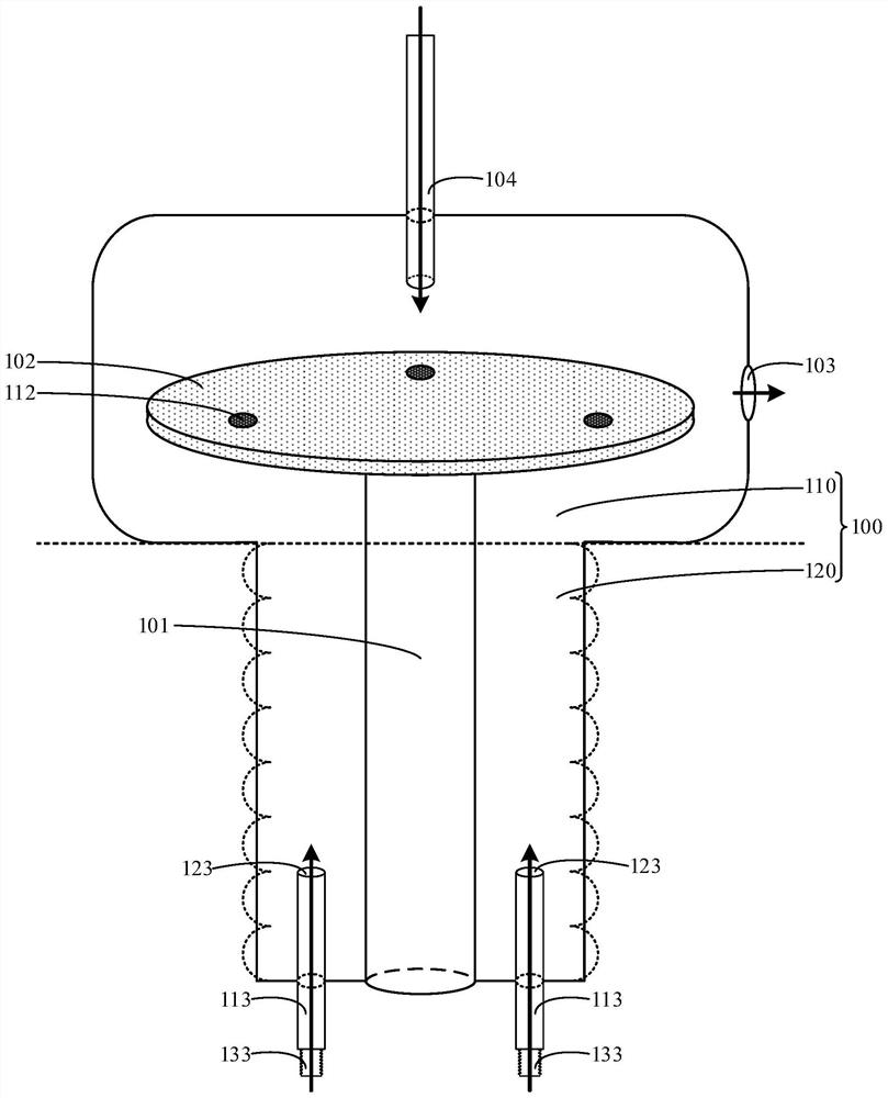
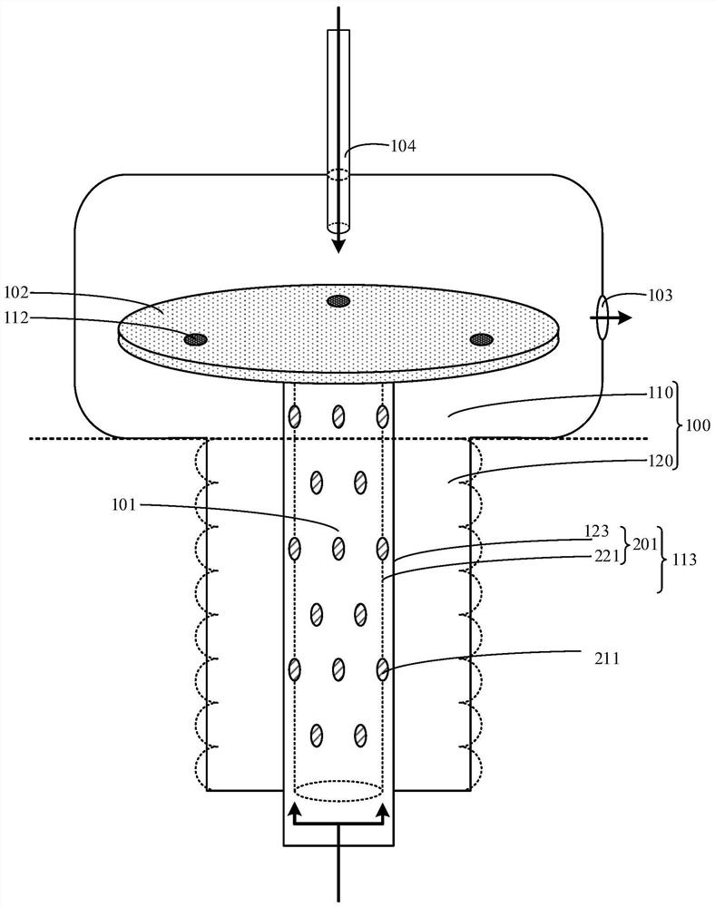
[0035] At present, the impurities accumulated at the bottom of the machine may rise up with the introduction of process gas during the production process, and fall on the wafer under the CVD process, contaminating the wafer product and directly causing the product to be scrapped.

[0036] In addition, impurities attached to the wafer may continue to contaminate other semiconductor chambers.

[0037] In order to ensure the deposition environment inside the CVD machine, the CVD machine is usually cleaned by the relevant staff during the maintenance of the CVD machine to remove the deposited impurities inside the machine. When the CVD machine performs the process for a long time , a large amount of impurities will accumulate at the bottom of the machine, which will shorten the maintenance cycle of the CVD machine, and the maintenance of the CVD machine will consume a lot of time, thereby reducing the production efficiency of wafer products.

[0038] In order to solve the above pr...


PUM

PropertyMeasurementUnit
widthaaaaaaaaaa

Abstract

The embodiment of the invention provides semiconductor equipment and a cleaning system.The semiconductor equipment comprises an equipment cavity, a supporting column and a bearing table, the supporting column and the bearing table are located in the equipment cavity, and the supporting column is used for supporting the bearing table; the gas outlet, the first gas inlet assembly and the second gas inlet assembly are arranged on the equipment cavity, the first gas inlet assembly and the second gas inlet assembly are used for introducing clean gas into the equipment cavity, and the gas outlet is used for discharging gas in the equipment cavity; the first air inlet assembly and the second air inlet assembly are arranged on the equipment cavities on the upper side and the lower side of the bearing face of the bearing table correspondingly, one of the first air inlet assembly and the second air inlet assembly is used for cleaning the equipment cavity, away from the supporting column, of the bearing face, and the other one is used for cleaning a gap between the supporting column and the equipment cavity. According to the embodiment of the invention, the bottom gap of the machine table can be cleaned under the condition that the machine table is not shut down, so that the cleaning operation of the machine table is completed on the premise that the production efficiency of products is not reduced.

Description

technical field [0001] The present invention relates to the field of semiconductor manufacturing process, in particular to a semiconductor equipment and a cleaning system. Background technique [0002] The Chemical Vapor Deposition (CVD) process is widely used in the semiconductor manufacturing process. At present, the chemical vapor deposition process is usually performed by a CVD machine. Due to the design defects of the original CVD machine, the cleaning gas during the process is produced by the CVD machine. The top of the CVD machine is passed through, so as to clean the CVD machine, but it is difficult for the cleaning gas to clean the bottom gap of the CVD machine, which leads to the accumulation of a large amount of impurities at the bottom of the CVD machine after a long-term process flow. [0003] The impurities accumulated at the bottom of the machine may rise up with the introduction of process gas during the production process and fall on the wafer under the CVD ...

Claims


Application Information

Patent Timeline
Patent Type & Authority Applications(China)
IPC IPC(8): C23C16/44
CPCC23C16/4405C23C16/44
Inventor 郭超
Owner CHANGXIN MEMORY TECH INC
Why Eureka
Try Eureka