Method and circuit for reducing idle loss of switch power supply

A technology of no-load loss and switching power supply, which is applied in the electronic field, can solve the problems of output jump and no-load loss that are difficult to reduce, and achieve the effect of reducing the drive

Inactive Publication Date: 2009-07-08
檀明升
View PDF0 Cites 4 Cited by
  • Summary
  • Abstract
  • Description
  • Claims
  • Application Information

AI Technical Summary

Problems solved by technology

Some of this method will produce output jump (or down frequency) ripple at light load, and it is difficult to reduce the no-load loss at high voltage to a lower level

Method used


Image

  • Method and circuit for reducing idle loss of switch power supply
  • Method and circuit for reducing idle loss of switch power supply
  • Method and circuit for reducing idle loss of switch power supply

Examples


Embodiment Construction

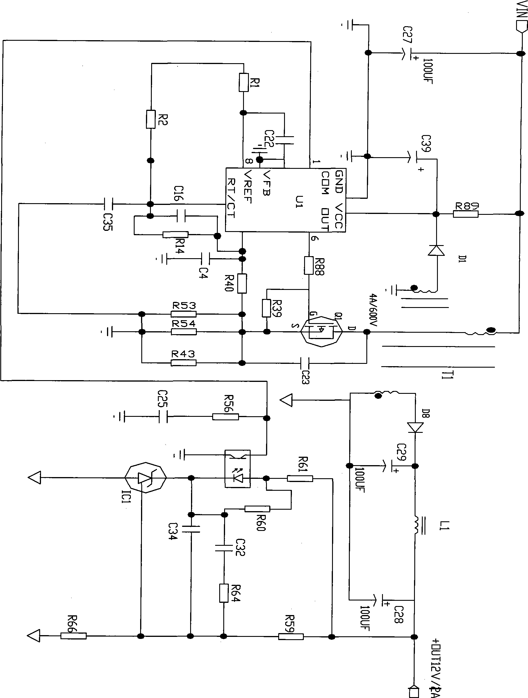
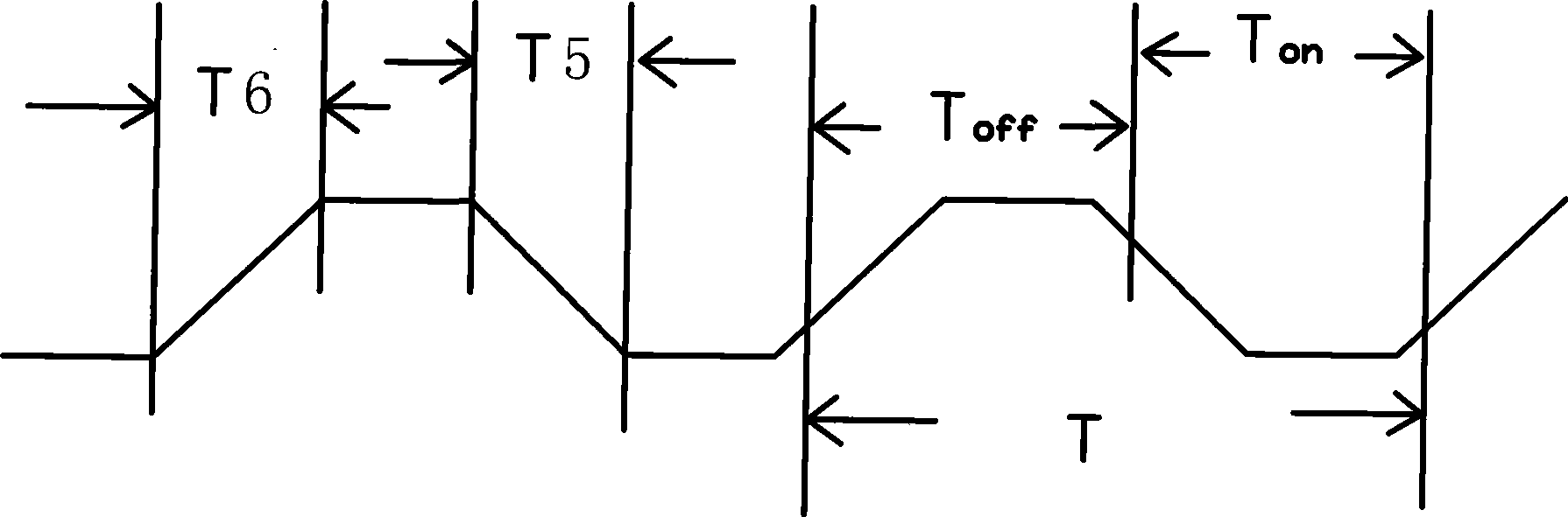
[0027] The embodiment of the present invention provides a method and circuit for reducing the no-load loss of the switching power supply, controlling the driving waveform of the chip U1 in the switching power supply, so that the power switching element Q1 completes the switching process of the power switch Q1 within the turn-on time T5.

[0028] In order to better understand the technical solutions provided by the embodiments of the present invention, the embodiments provided by the present invention will be described in detail below in conjunction with the accompanying drawings.

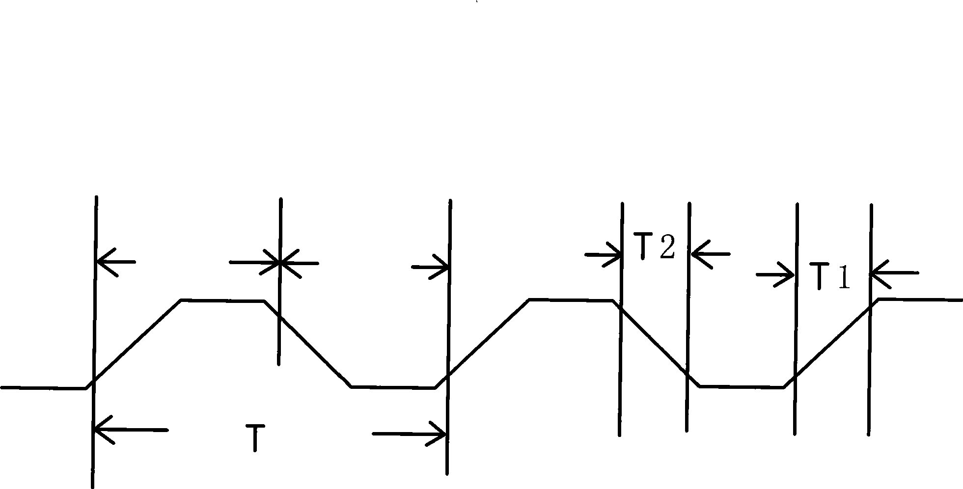
[0029] see figure 2 with Figure 4 , the purpose of the present invention can be achieved by using the on-duty ratio D of the power supply.

[0030] In the case of no load, set the on-duty ratio as D1, use D1=Ton / T to deduce Ton=D1 / F. As long as the switching frequency F of the power switching element Q1 is increased at no-load, the on-time Ton of the power switching element Q1 is shorter than th...


PUM


Abstract

The embodiment of the invention relates to the field of switching power supplies, and provides a method and a circuit for reducing the open circuit loss of a switching power supply. By controlling the driving waveform of a chip U1 in the switching power supply, the invention leads a power switching element Q1 to complete the switching-on process of the power switching element Q1 within a turn-on time T5. The invention can enable the power switching element Q1 is to work in a semi-conducting state, thereby reducing the loss for driving, switching on as well as switching off and conducting the power switching element Q1.

Description

technical field [0001] Embodiments of the present invention relate to the electronic field, and in particular to a method for reducing no-load loss of a switching power supply. Background technique [0002] Power supplies in the prior art, such as inverter power supplies and switching power supplies, will lose power when they are no-load. For example, the working principle of switching power supplies is as follows: figure 1 As shown, the input electric energy is transmitted to the output by turning on and off the power switch element Q1, generally the input is AC (or DC), and the output is DC. The required output voltage is achieved by controlling the turn-on and cut-off time of the power switch element Q1, and the power switch element Q1 is turned on by the output high level of the drive pin 6 of the control chip (such as UC3842) U1, and the output is low level to As of Q1, if image 3 As shown, it is the ideal waveform for the output of pin 6 to drive the level of Q1. A...

Claims


Application Information

Patent Timeline
Patent Type & Authority Applications(China)
IPC IPC(8): H02M3/335H02M1/00
Inventor 檀明升
Owner 檀明升
Why Eureka
Try Eureka