Plasma treatment apparatus

A plasma and processing device technology, applied in the field of microelectronics, can solve the problems of poor adaptability, inability to realize plasma density adjustment, inability to meet various processing techniques, etc., and achieve the effect of improving adaptability

Inactive Publication Date: 2009-07-08
BEIJING NAURA MICROELECTRONICS EQUIP CO LTD
View PDF0 Cites 35 Cited by
  • Summary
  • Abstract
  • Description
  • Claims
  • Application Information

AI Technical Summary

Problems solved by technology

[0018] Therefore, the above-mentioned plasma processing device in the prior art can only meet the requirements of a few processing techniques, but cannot realize the adjustment of the plasma density in a wide range; therefore, its adaptability is poor, and it cannot meet the requirements of various processing techniques. craft needs

Method used


Image

  • Plasma treatment apparatus
  • Plasma treatment apparatus
  • Plasma treatment apparatus

Examples


Embodiment approach

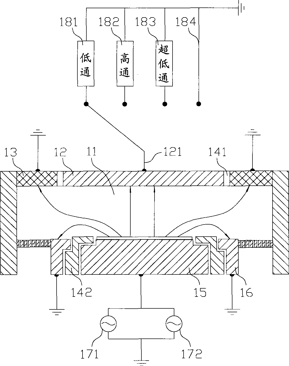
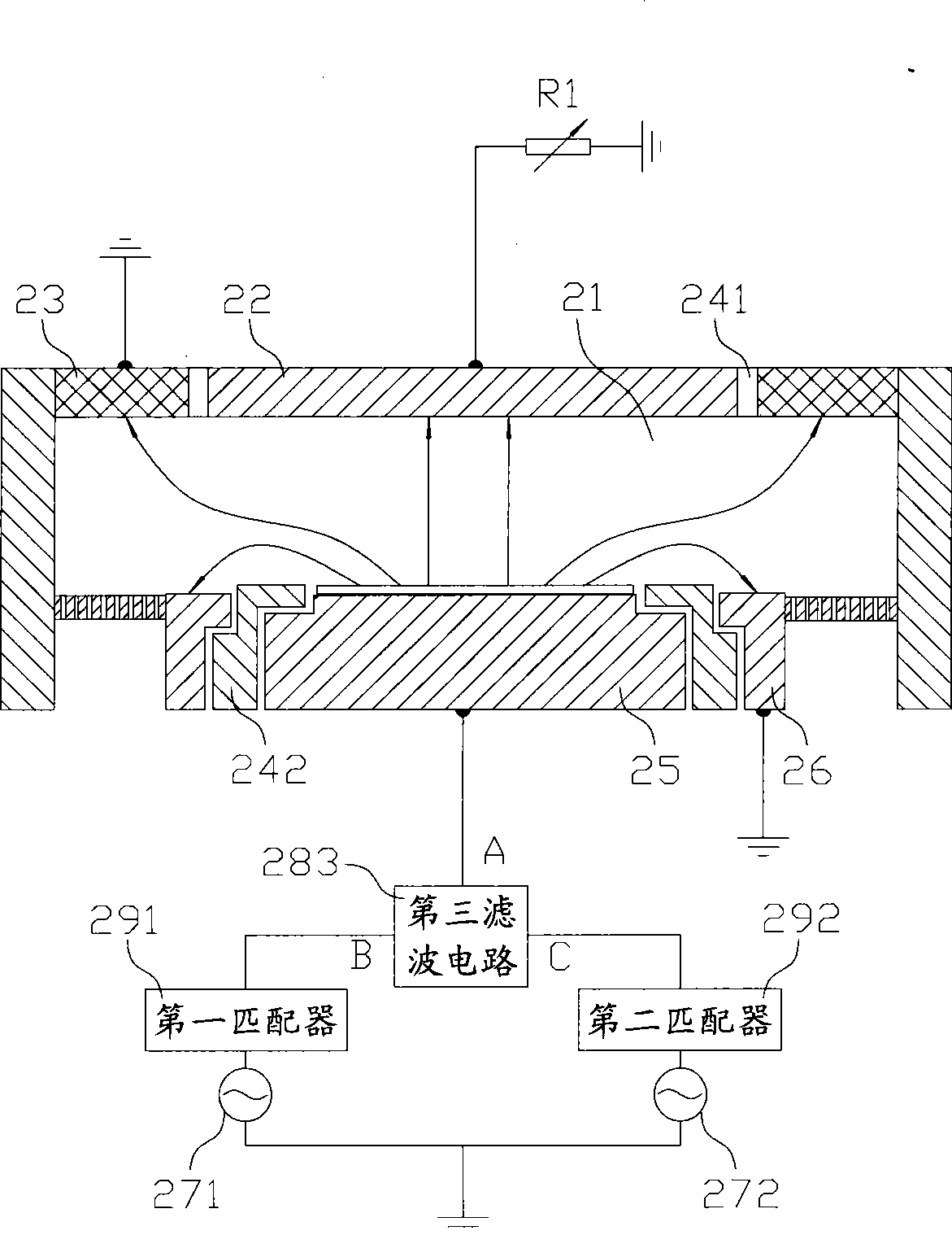
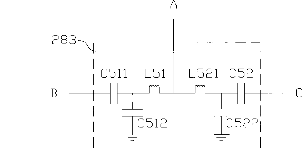
[0071] In the second specific implementation manner, the plasma processing apparatus provided by the embodiment of the present invention is further improved on the basis of the above-mentioned first specific implementation manner.

[0072] As mentioned above, in order to broaden the adaptability of the plasma processing apparatus, it should be possible to adjust the relevant parameters of the plasma in the reaction chamber 21 , and the relevant parameters generally involve density, energy, flow rate and the like. Usually, the adjustment of plasma energy is realized through the first radio frequency power supply 271 ; the adjustment of plasma density is realized through the second radio frequency power supply 272 .

[0073] When adjusting the above parameters in order to adapt to different processes, it is best to control the density and energy of the plasma separately; however, due to the coupling between the first radio frequency power supply 271 and the second radio frequency...


PUM


Abstract

The invention discloses a plasma treatment device, which comprises oppositely arranged radio frequency driving electrode (25) and a passive electrode (22); the passive electrode (22) is encircled by a first grounding ring (23), which are insulated from each other; the radio frequency driving electrode (25) is encircled by a second grounding ring (23), which are insulated from each other; the radio frequency driving electrode (25) is connected respectively with a first radio frequency power source (271) and a second radio frequency power source (272); a first impedance regulating element is connected in series between the passive electrode (22) and a ground wire. The plasma treatment device provided by the invention overcomes a shortcoming of the current technology that energy of plasma can be converted only among several specific isolated values, and more craft processes required by different plasma density can be realized in the same reaction chamber.

Description

technical field [0001] The invention relates to the technical field of microelectronics, in particular to a plasma processing device. Background technique [0002] Plasma processing equipment is processing equipment widely used in the field of semiconductor manufacturing. [0003] Please refer to figure 1 , figure 1 It is a schematic structural diagram of a typical plasma processing device in the prior art. [0004] A plasma processing device generally includes a casing (no reference numerals are added in the figure), in which a reaction chamber 11 is located. The top of the reaction chamber 11 is provided with a passive electrode 12 and an upper ground ring 13 surrounding the passive electrode 12 ; the two are separated by a first insulating ring 141 . The bottom of the reaction chamber 11 is provided with a radio frequency driving electrode 15 and a lower ground ring 16 surrounding the radio frequency driving electrode 15 , which are separated by a second insulating ri...

Claims


Application Information

Patent Timeline
Patent Type & Authority Applications(China)
IPC IPC(8): H05H1/46H01L21/00
CPCH01J37/32623H01J37/32174H01J37/32577H01J37/32091H01J37/32642
Inventor 南建辉宋巧丽
Owner BEIJING NAURA MICROELECTRONICS EQUIP CO LTD
Why Eureka
Try Eureka