Method for detecting polychlorinated biphenyl by using silver nanometer tree branches and leaves
A polychlorinated biphenyl and silver nanotechnology, applied in the direction of Raman scattering, material excitation analysis, etc., can solve the problems of increased detection complexity, inability to detect PCBs, and failure to prepare PCBs, etc., to achieve detection The process is simple and the detection accuracy guarantees the effect
- Summary
- Abstract
- Description
- Claims
- Application Information
AI Technical Summary
Problems solved by technology
Method used
Image
Examples
preparation example Construction
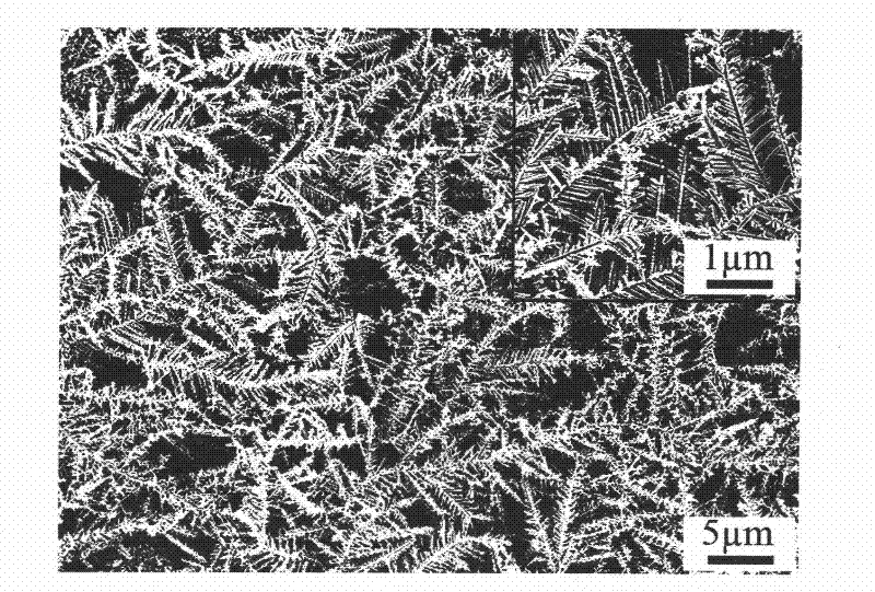
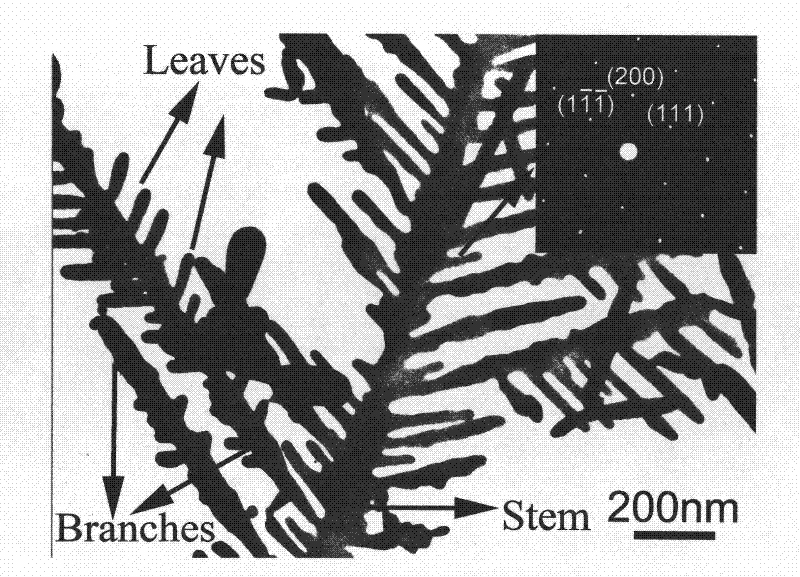
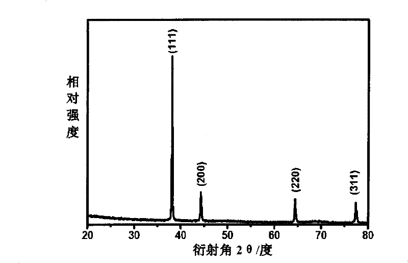
[0018] The preparation method of silver nano-branches and leaves is as follows: first place the silicon chip in a mixed solution of hydrofluoric acid with a concentration of 3-7M and silver nitrate with a concentration of 0.01-0.03M, and react at a temperature of 45-55°C for 5-60min , A film with a thickness ≥ 1.5 μm and composed of numerous nano-branches is obtained on a silicon wafer. The nano-branches and leaves in the film are as figure 1 , figure 2 shown and image 3 Silver nano-branches and leaves with a hierarchical structure of trunks, branches and leaves shown in the curve, wherein the length of the trunk is 1-10 μm and the diameter is 10-100 nm, the length of the branches is 100 nm-10 μm and the diameter is 10-100 nm, The length of the leaves is 10 nm to 1 μm, and the diameter is 10 to 100 nm.
[0019]PCBs are PCB4, PCB17, PCB18, PCB30, PCB44, PCB49, PCB66, PCB74, PCB77, PCB82, PCB95, PCB96, PCB99, PCB103, PCB105, PCB110, PCB128, PCB132, PCB136 and all the rest. ...
Embodiment 1
[0023] The specific steps of detection are: step 1, using a wavelength of 450-550nm and a power density of 1×10 5 W / cm 2 The laser is used as a light source to irradiate the silver nanofilm adsorbed on polychlorinated biphenyls on the focal plane of the microscope of the confocal microscope Raman test system; wherein the laser source is an argon ion laser with a wavelength of 488.0nm (or 514.5nm), Polychlorinated biphenyls are PCB77, one of its isomers, which is made by placing silver nano-films at a concentration of 10 -6 M's PCB77 is soaked in the n-hexane solution and then dried. The thickness of the silver nano film is 1.5 μm, and it is composed of silver nano branches and leaves. The length of the silver nano branches and leaves trunk is 1 μm, and the diameter is 10nm. The diameter is 10nm, the length of the leaf is 10nm, and the diameter is 10nm. Step 2, scan the Raman scattering signal of the silver nano film, and perform data integration on the collected scanning sig...
Embodiment 2
[0025] The specific steps of detection are: step 1, using a wavelength of 450-550nm and a power density of 3×10 5 W / cm 2 The laser is used as a light source to irradiate the silver nanofilm adsorbed on polychlorinated biphenyls on the focal plane of the microscope of the confocal microscope Raman test system; wherein the laser source is an argon ion laser with a wavelength of 488.0nm (or 514.5nm), Polychlorinated biphenyls are PCB77, one of its isomers, which is made by placing silver nano-films at a concentration of 10 -7 M's PCB77 is soaked in the n-hexane solution and then dried. The thickness of the silver nano film is 1.7 μm, and it is composed of silver nano branches and leaves. The length of the silver nano branches and leaves trunk is 3 μm, and the diameter is 30nm. The diameter is 30 nm, the length of the leaf is 50 nm, and the diameter is 30 nm. Step 2, scan the Raman scattering signal of the silver nano film, and perform data integration on the collected scanning ...
PUM
| Property | Measurement | Unit |
|---|---|---|
| length | aaaaa | aaaaa |
| diameter | aaaaa | aaaaa |
| length | aaaaa | aaaaa |
Abstract
Description
Claims
Application Information


