Dielectric material for plasma display panel
A technology of dielectric materials and display panels, applied in circuits, discharge tubes, electrical components, etc., to achieve the effect of excellent transparency
- Summary
- Abstract
- Description
- Claims
- Application Information
AI Technical Summary
Problems solved by technology
Method used
Image

Examples
Embodiment
[0066] The dielectric material of the plasma display panel of the present invention will be specifically described below according to the embodiments.
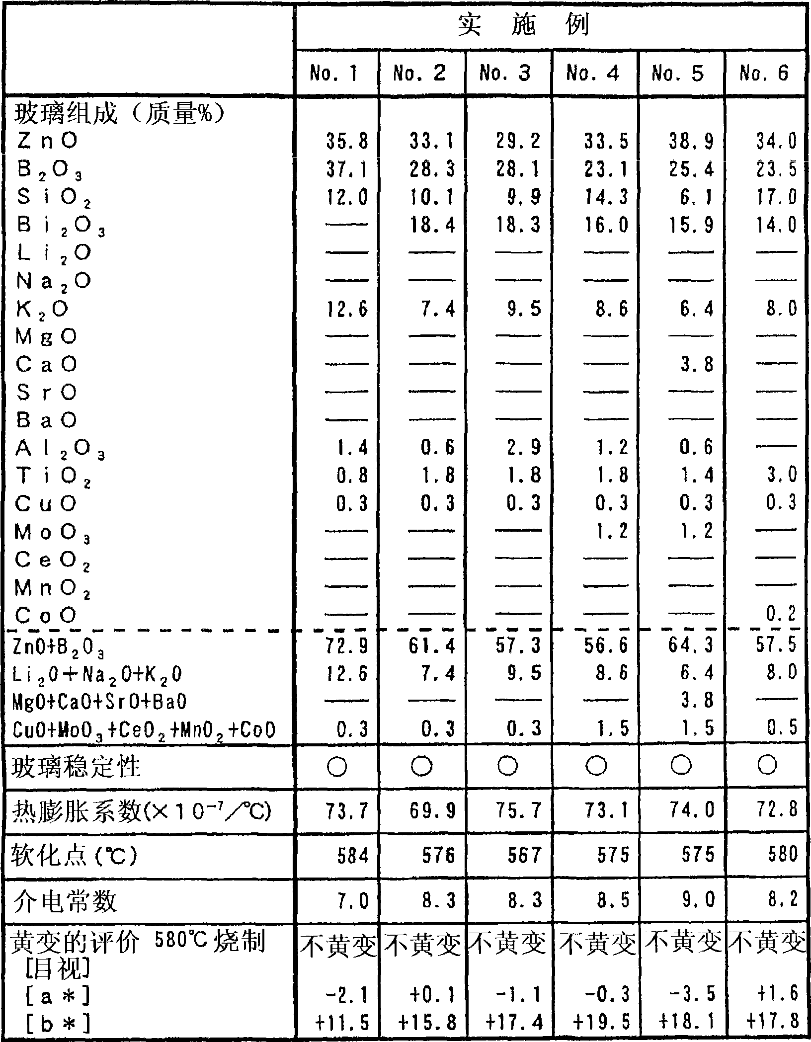
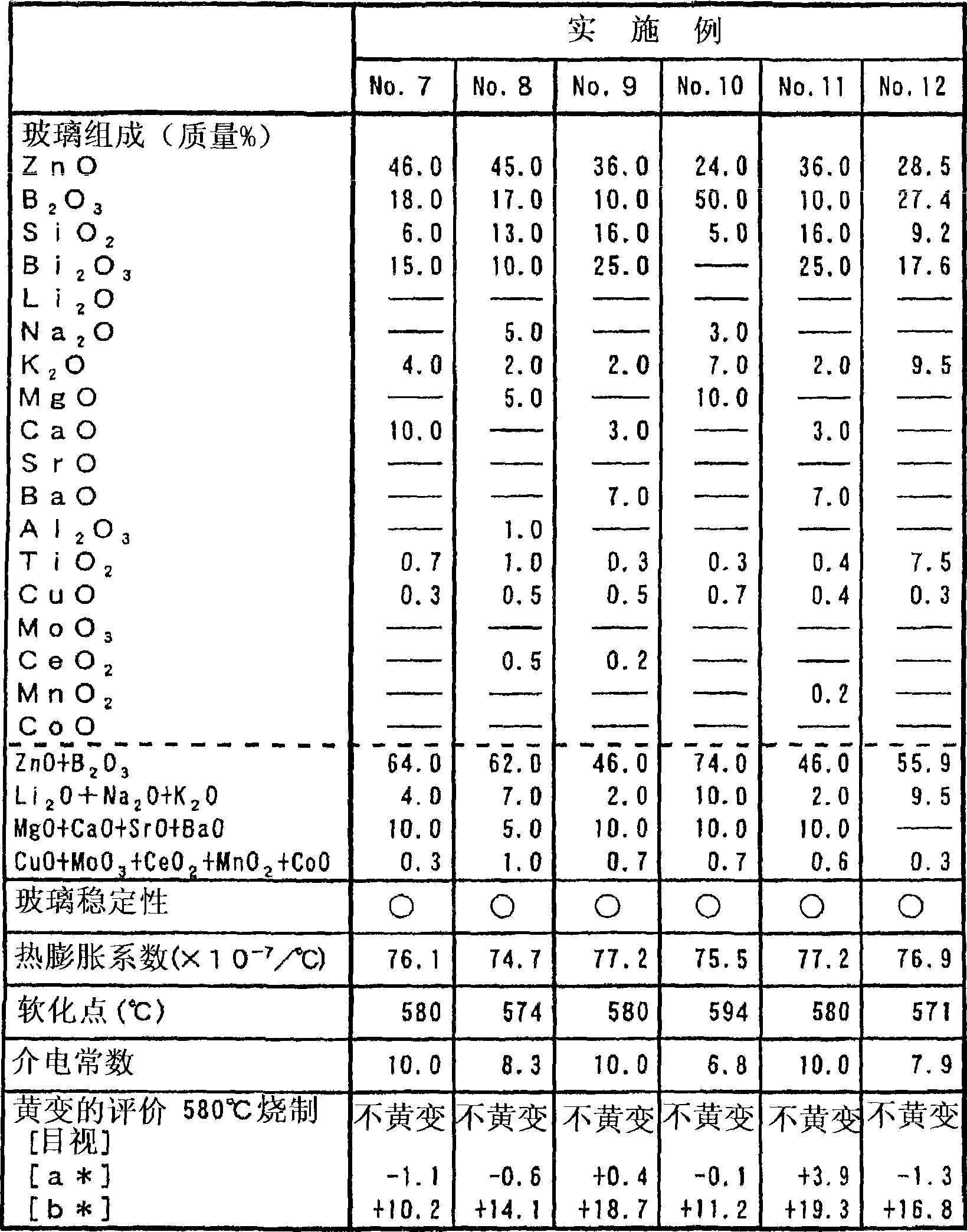
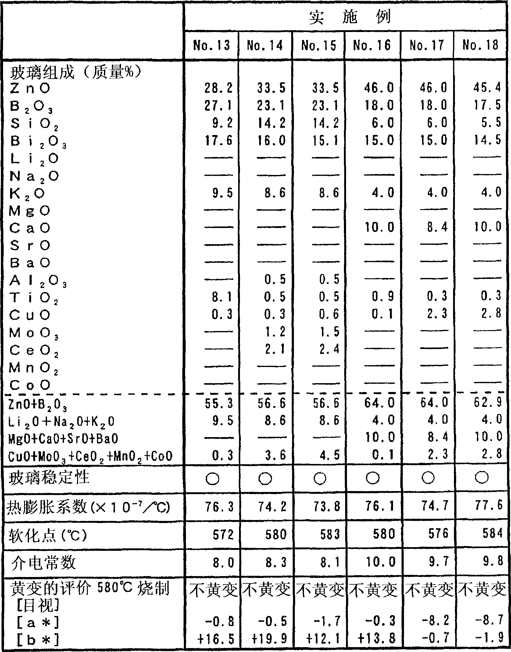
[0067] Tables 1 to 5 show examples (sample Nos. 1 to 19) and comparative examples (sample Nos. 20 to 26) of the present invention, respectively. In addition, sample No. 20 represents the ZnO-B 2 o 3 class of materials.
[0068] Table 1
[0069]
[0070] Table 2
[0071]
[0072] table 3
[0073]
[0074] Table 4
[0075]
[0076] table 5
[0077]
[0078] Each sample in the table was prepared as follows.
[0079] First, raw materials were mixed and homogenized according to the glass composition shown in the table in mass %. Next, it was placed in a platinum crucible and melted at 1300° C. for 2 hours, and then the molten glass was molded into a thin plate shape. Then, it is pulverized with a ball mill and air-flow classified to obtain the average particle diameter D 50 Below 3.0μm, maximum particle siz...
PUM
 Abstract
Description
Claims
Application Information
 - Generate Ideas
- Intellectual Property
- Life Sciences
- Materials
- Tech Scout
- Unparalleled Data Quality
- Higher Quality Content
- 60% Fewer Hallucinations
Browse by: Latest US Patents, China's latest patents, Technical Efficacy Thesaurus, Application Domain, Technology Topic, Popular Technical Reports.
© 2025 PatSnap. All rights reserved.Legal|Privacy policy|Modern Slavery Act Transparency Statement|Sitemap|About US| Contact US: help@patsnap.com