Automatic sorting machine for semiconductor chip

An automatic sorting and semiconductor technology, applied in semiconductor/solid-state device manufacturing, semiconductor/solid-state device testing/measurement, electrical components, etc., can solve problems affecting sorting quality, sorting accuracy and reliability, and achieve The effect of improving accuracy and reliability

Inactive Publication Date: 2009-09-23
常州新区爱立德电子有限公司
View PDF0 Cites 28 Cited by
  • Summary
  • Abstract
  • Description
  • Claims
  • Application Information

AI Technical Summary

Problems solved by technology

Then use special equipment to detect the chip, record the position of the chip and the corresponding detection parameters, and then expand the chip and transfer it to a special sorting machine for sorting according to the position and detection parameters rec

Method used


Image

  • Automatic sorting machine for semiconductor chip
  • Automatic sorting machine for semiconductor chip
  • Automatic sorting machine for semiconductor chip

Examples


Embodiment Construction

[0016] The present invention will now be described in further detail in conjunction with the accompanying drawings and preferred embodiments. These drawings are all simplified schematic diagrams, which only illustrate the basic structure of the present invention in a schematic manner, so they only show the configurations related to the present invention.

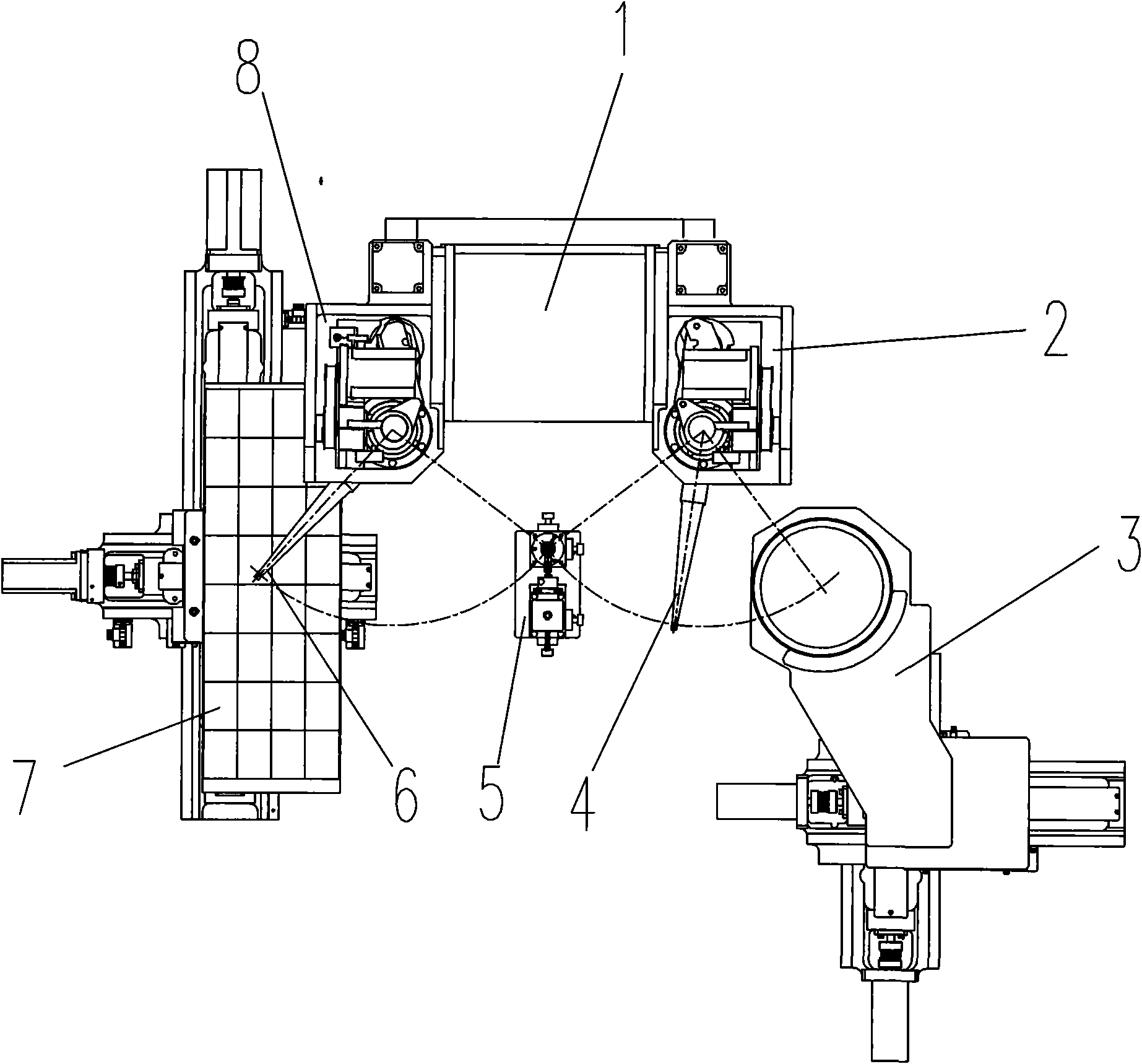
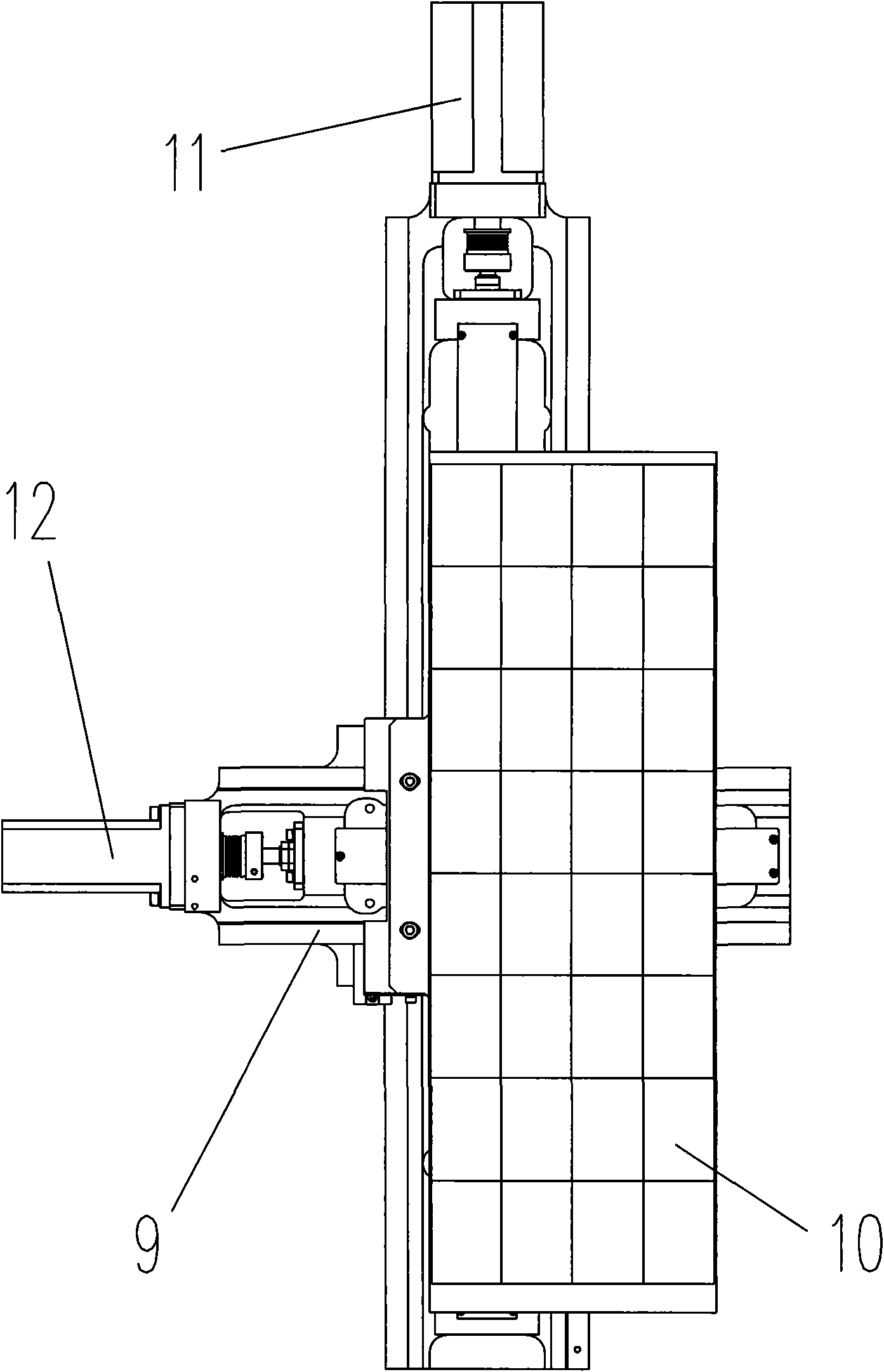
[0017] Such as figure 1 As shown, the chip feeder 3 is installed on the bottom plate, such as image 3 As shown, the chip placement platform is installed on the two-dimensional platform 14, and the two-dimensional platform 14 is driven by the motor 14 and the motor 16 respectively, so as to realize the movement of the two-dimensional platform in the two-dimensional plane, and then drive the chip placement platform 13 to move to a specified position. Location. The chip on the chip placement platform 13 is identified by the CCD camera installed above the chip placement platform 13, and the position difference information is ...


PUM


Abstract

The invention discloses an automatic sorting machine for semiconductor chips, comprising a bottom plate. The bottom plate is provided with a chip feeding table, a chip test table, a chip BIN sorting table and a material taking unit. The transfer of a chip is carried out between the chip feeding table and the chip test table as well as between the chip test table and the chip BIN sorting table through the material taking unit. The design of integrating examining, test and sorting greatly improves the accuracy and the reliability of examining and sorting of the semiconductor chips, and avoids the condition that concentrated examining is firstly carried out and then BIN is singly sorted to be easy to cause errors so as to influence the accuracy of the sorting.

Description

technical field [0001] The invention relates to the testing of semiconductor chips, in particular to an automatic semiconductor chip sorting machine for detecting and classifying optical and electrical parameters of semiconductor chips. Background technique [0002] The semiconductor chip manufacturing process is complex, and the control of the process has a great impact on the quality of the chip. A complete semiconductor chip manufacturing can be roughly divided into initial chip design and wafer manufacturing, mid-term wafer testing and packaging, and later final testing and product shipment. In every link, it is hoped that the characteristics and quality of semiconductor chips can be detected accurately and reliably. [0003] At present, the commonly used detection method is to carry out detection and classification after the chip packaging is completed. Since the detection is not carried out in the early stage, the unqualified chips are also packaged. After cutting th...

Claims


Application Information

Patent Timeline
IPC IPC(8): H01L21/66H01L21/683
Inventor 王琳唐国强陈云顾方成沈国平
Owner 常州新区爱立德电子有限公司
Why Eureka
Try Eureka