Supercharge Your Innovation With Domain-Expert AI Agents!

Active matrix display device with optical feedback and driving method thereof

A display device and active matrix technology, applied in the field of active matrix electroluminescent display devices, can solve the problems of increasing the limit of the circuit

Inactive Publication Date: 2009-09-23
KONINK PHILIPS ELECTRONICS NV
View PDF4 Cites 6 Cited by
  • Summary
  • Abstract
  • Description
  • Claims
  • Application Information

AI Technical Summary

Problems solved by technology

However, there is still a need to provide increased circuit limits for aging of circuit components, including changes in the threshold voltage of drive transistors, as well as aging of display elements and characteristic changes of other components in the circuit.

Method used


Image

  • Active matrix display device with optical feedback and driving method thereof
  • Active matrix display device with optical feedback and driving method thereof
  • Active matrix display device with optical feedback and driving method thereof

Examples


Embodiment Construction

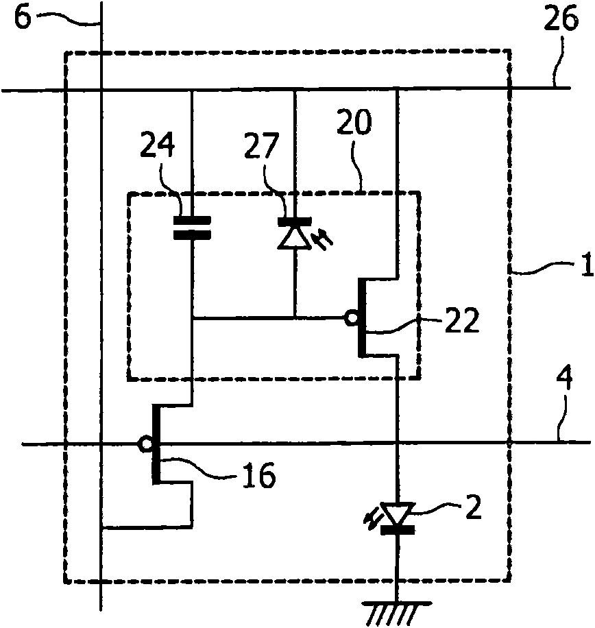
[0071] Figure 3 shows an example of a "snap" pixel schematic as disclosed in WO 04 / 084168.

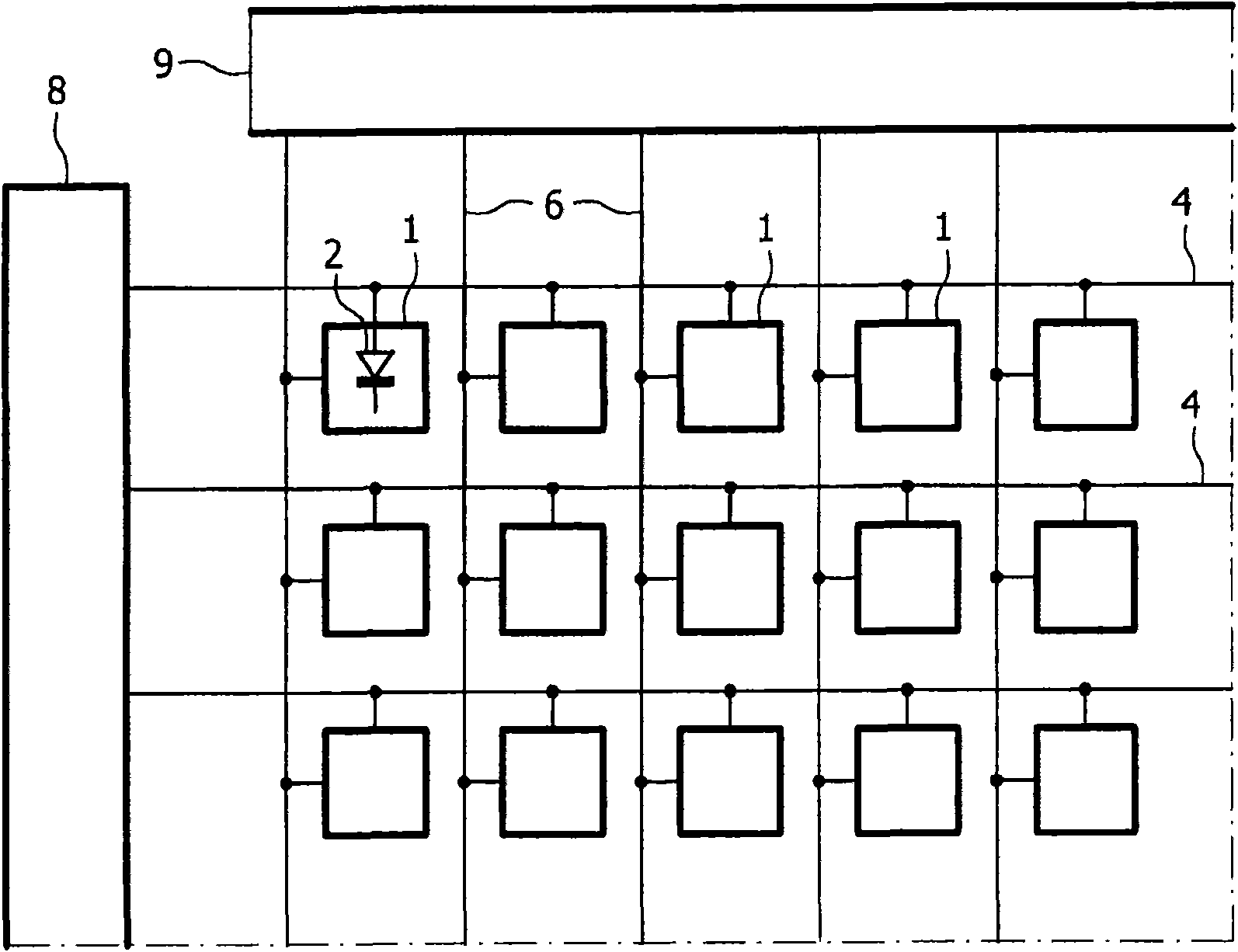
[0072] Using the same reference numerals to designate the same components as in FIG. 2 , pixel circuits are used in a display such as that shown in FIG. 1 . The circuit of Figure 3 is suitable for implementation using amorphous silicon n-type transistors.

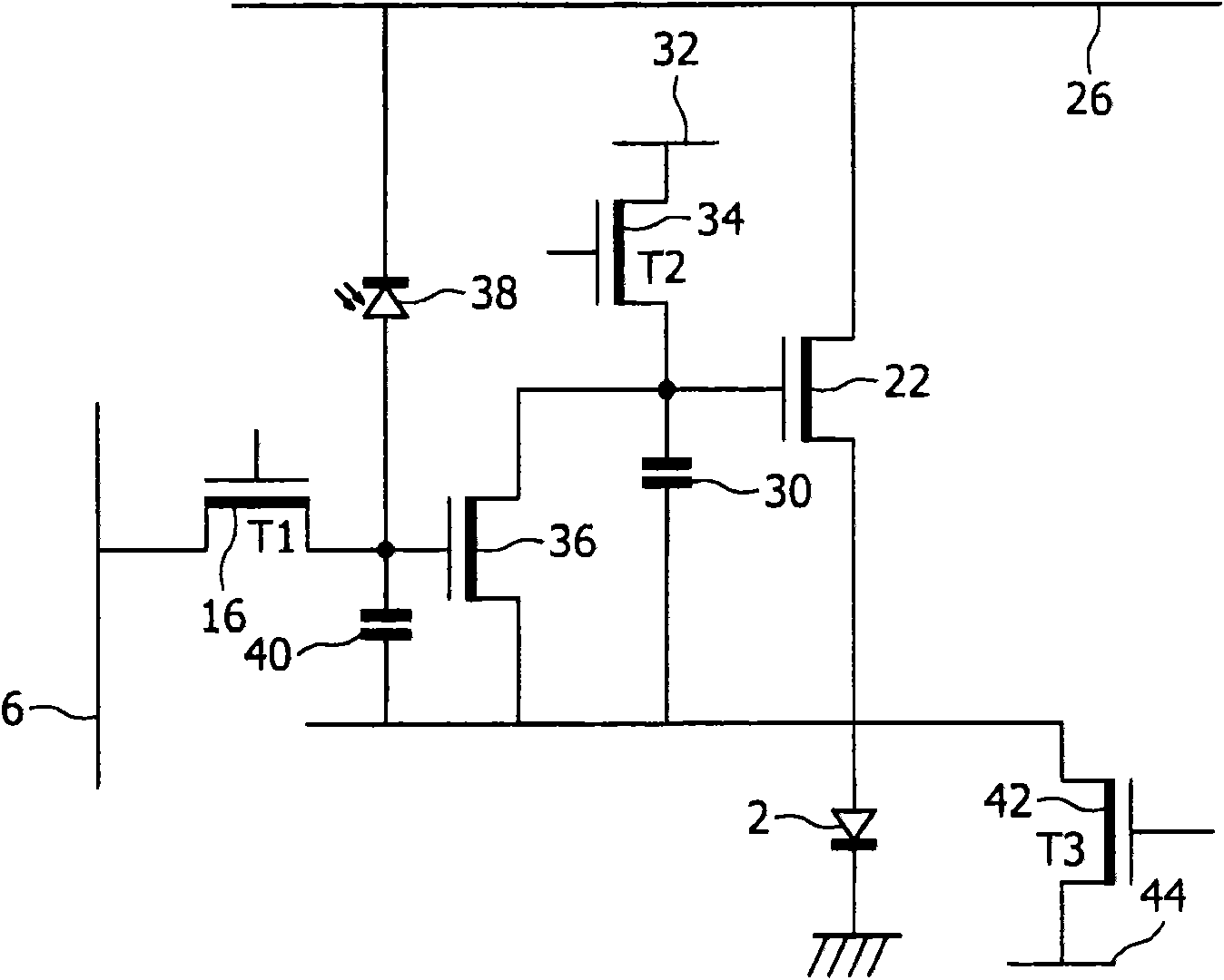
[0073] The gate-source voltage of the drive transistor 22 is again maintained on the storage capacitor 30 . The capacitor is charged to a fixed voltage from a charging line 32 by means of a charging transistor 34 (T2). Thus, the drive transistor 22 is driven to a constant level independent of the data input to the pixel when the display element is illuminated. Brightness is controlled by varying the duty cycle, especially by varying the time the drive transistor is turned off.

[0074] The drive transistor 22 is switched off by means of the discharge transistor 36 , which discharges the storage capacitor 30 . When the discharge ...


PUM


Abstract

An active matrix display device comprises an array of display pixels, each pixel comprising a current-driven light emitting display element (2), a drive transistor (22) for driving a current through the display element (2) and a storage capacitor (30) for storing a voltage to be used for addressing the drive transistor (22). A discharge transistor (36) is used for discharging the storage capacitor (30) thereby to switch off the drive transistor in dependence on the light output of the display element (2). Reading circuitry (70) is used for monitoring the charge on a discharge capacitor (40), the pixel data is corrected in response to the reading circuitry measurements. This can extend the lifetime of the display.

Description

technical field [0001] The present invention relates to an active matrix display device, in particular (but not exclusively) to an active matrix electroluminescent display device having a thin film switching transistor associated with each pixel. Background technique [0002] Matrix display devices using electroluminescent light-emitting display elements are known. The display elements may comprise, for example, organic thin film electroluminescent elements using polymer materials, or light emitting diodes (LEDs) using conventional III-V semiconductor compounds. The recent development of organic electroluminescent materials, especially polymeric materials, has demonstrated their ability to be practically used in video display devices. These materials generally comprise one or more layers of a semiconducting conjugated polymer sandwiched between a pair of electrodes, one of which is transparent and the other electrode is of a material suitable for injecting holes or electron...

Claims


Application Information

Patent Timeline
Patent Type & Authority Applications(China)
IPC IPC(8): G09G3/32
CPCG09G3/3258G09G2320/045G09G2300/0852G09G3/3291G09G2320/0295G09G2300/0861G09G2320/043G09G3/2014G09G2300/043G09G2320/0233G09G2320/0238G09G2300/0819G09G2310/0297G09G2360/148G09G3/32G09G3/20
Inventor D·A·菲什S·C·迪恩N·布拉曼特
Owner KONINK PHILIPS ELECTRONICS NV
Features
  • R&D
  • Intellectual Property
  • Life Sciences
  • Materials
  • Tech Scout
  • Unparalleled Data Quality
  • Higher Quality Content
  • 60% Fewer Hallucinations
Learn More