Semiconductor device

一种半导体、偏置电路的技术,应用在半导体器件、半导体/固态器件制造、晶体管等方向,能够解决难以制造半导体装置、变动等问题,达到降低噪声的影响、稳定产生的效果

Inactive Publication Date: 2009-09-30
SEMICON ENERGY LAB CO LTD
View PDF4 Cites 6 Cited by
  • Summary
  • Abstract
  • Description
  • Claims
  • Application Information

AI Technical Summary

Problems solved by technology

[0005]Since semiconductor devices capable of wireless communication include integrated circuits provided with tiny semiconductor elements, there are problems such as fluctuations, and it is difficult to manufacture semiconductor devices with ideal electrical characteristics

Method used


Image

  • Semiconductor device
  • Semiconductor device
  • Semiconductor device

Examples


Embodiment approach 1

[0066] This embodiment mode will describe a configuration example of a semiconductor device of the present invention in which a demodulation signal generation circuit is included with reference to the drawings.

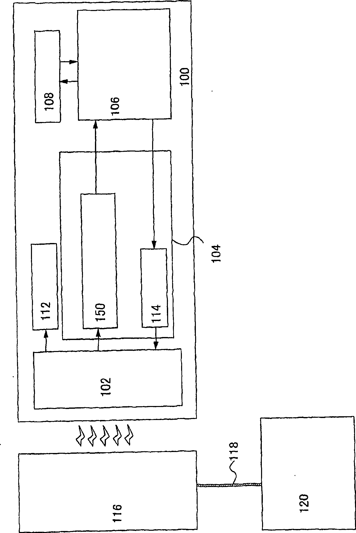
[0067] figure 2 A block diagram of a semiconductor device of the present invention is shown. The semiconductor device 100 of the present invention wirelessly transmits and receives data to and from the reader / writer 116 by electromagnetic waves. Reader / writer 116 is preferably connected to control device 120 via communication line 118 . The control device 120 controls communication between the reader / writer 116 and the semiconductor device 100 .

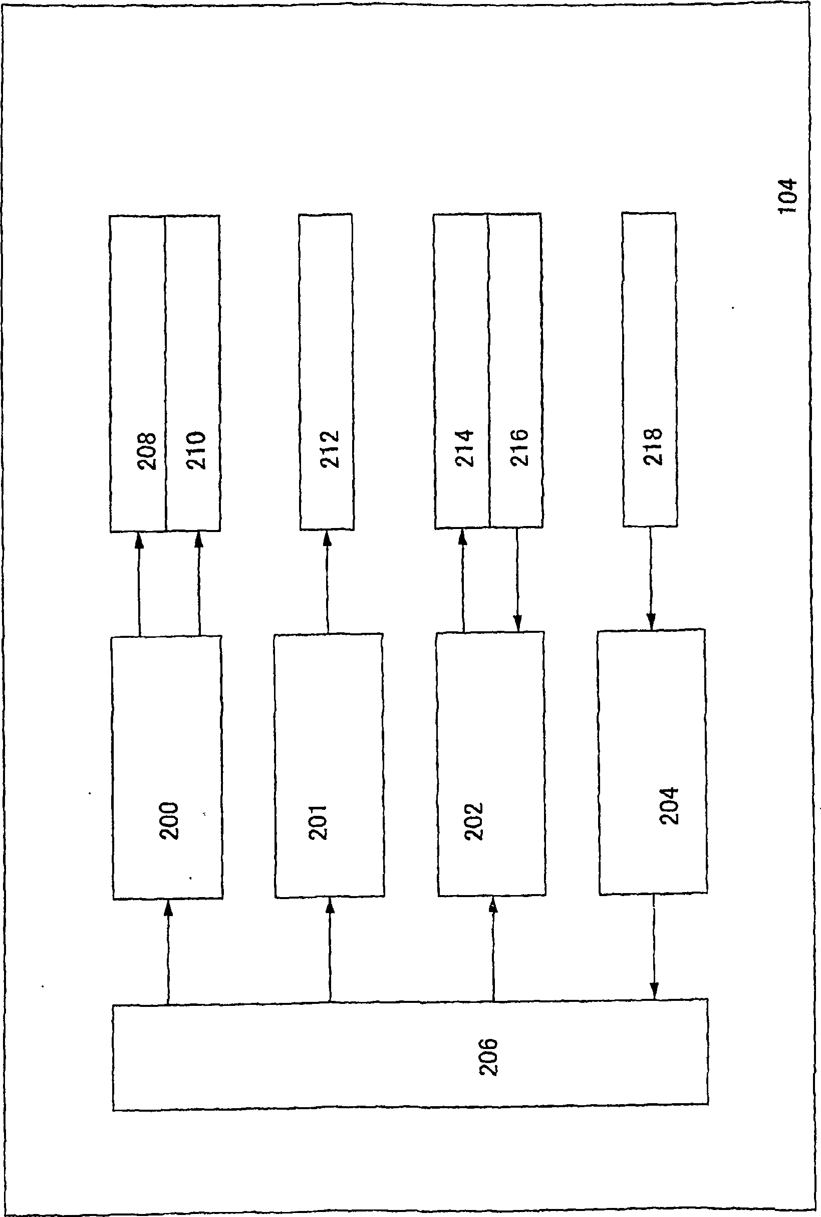
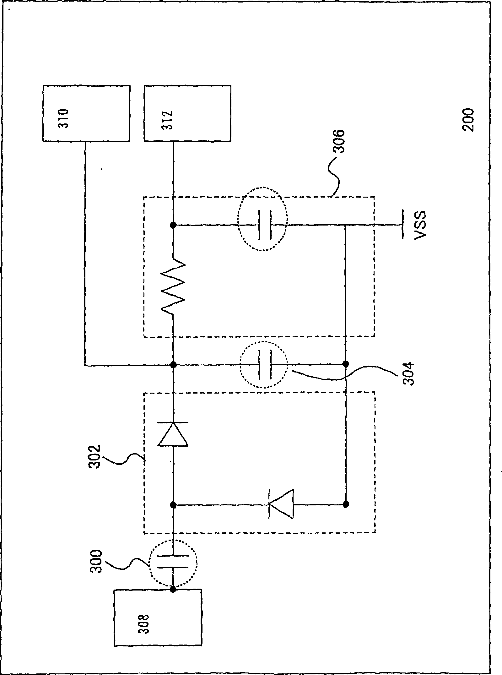
[0068] The semiconductor device 100 includes an antenna circuit 102 , a power supply circuit 112 , an analog circuit 104 , a digital circuit 106 , and a memory circuit 108 . The analog circuit 104 has a demodulation signal generation circuit 150 and a modulation circuit 114 . The semiconductor device 100 may not include...

Embodiment approach 2

[0112] This embodiment mode will describe a configuration example of a semiconductor device of the present invention including a demodulation signal generation circuit in a mode different from that of Embodiment Mode 1 with reference to the drawings. This embodiment mode will specifically describe a semiconductor device in the case of including a plurality of demodulation signal generation circuits, and selecting one demodulation signal generation circuit from among the plurality of demodulation signal generation circuits by a selection circuit at the time of operation.

[0113] Figure 31 A semiconductor device 1500 to which the present invention is applied is shown. exist Figure 31 Among them, the semiconductor device 1500 includes: an antenna circuit 102, which receives radio waves; an analog circuit 130, which generates power from a power supply from a signal received in the antenna circuit 102, and demodulates the signal; a digital circuit 106, which controls other circ...

Embodiment approach 3

[0173] This embodiment mode will describe a structural example of a semiconductor device including the demodulation signal generation circuit of the present invention in a different manner from Embodiment Modes 1 and 2. Specifically, this embodiment mode will employ a structure in which the semiconductor device described in Embodiment Mode 2 is provided with a battery.

[0174] Figure 14 A block diagram of the semiconductor device of this embodiment is shown. The semiconductor device 1800 of the present embodiment wirelessly transmits and receives data to and from the reader / writer 1811 by electromagnetic waves. The reader / writer 1811 is preferably connected to a control device 1813 through a communication line 1812 . The control device 1813 controls communication between the reader / writer 1811 and the semiconductor device 1800 .

[0175] In addition, the semiconductor device 1800 is wirelessly supplied with power from the reader / writer 1811 .

[0176] The semiconductor d...


PUM


Abstract

A demodulation signal is generated by provision of a demodulation signal generation circuit to the semiconductor device capable of wireless communication and by obtainment of a difference between voltages having opposite polarities by the demodulation signal generation circuit. Alternatively, a plurality of demodulation signal generation circuits and a selective circuit which selects a demodulation signal generation circuit depending on characteristics of a received signal are provided, where operation of a second demodulation signal generation circuit stops when a first demodulation signal generation circuit is operated. The selective circuit includes an inverter circuit, a flip-flop circuit, and a selector circuit. When the second demodulation signal generation circuit has a comparator and the like, power consumption thereof is reduced.

Description

technical field [0001] The present invention relates to semiconductor devices. In particular, the present invention relates to a semiconductor device capable of transmitting and receiving information using wireless communication without contact. Background technique [0002] In recent years, an individual identification technique in which individual identification information is given to an individual object to make information such as a history of an object clear has drawn attention. In particular, semiconductor devices capable of transmitting and receiving data using wireless communication through radio waves without contact have made great progress. Such a semiconductor device is called an ID tag, an RFID tag, or the like, and it has begun to be used for management of items in the market, and the like. [0003] In general, many objects called RFID tags or the like that have been put into practical use include an element forming layer and an antenna layer having a circui...

Claims


Application Information

Patent Timeline
Patent Type & Authority Applications(China)
IPC IPC(8): G06K19/07H01L27/08H01L21/822H01L27/088H01L21/8234H03D1/10H01L27/04H04B5/02
CPCG06K19/0702G06K19/07786G06K19/0723H04B5/0062H04B5/77G06K19/07H01L21/822H01L27/04H04B5/48
Inventor 热海知昭小林英智
Owner SEMICON ENERGY LAB CO LTD
Why Eureka
Try Eureka