Method for detecting surface leakage channel of semiconductor detection device under illumination

A device surface and light detection technology, applied in the direction of measuring electricity, measuring electrical variables, instruments, etc., can solve the problems of providing information, inability to distinguish surface leakage and internal leakage, and device performance impact

Active Publication Date: 2009-10-07
SHANGHAI INST OF TECHNICAL PHYSICS - CHINESE ACAD OF SCI
View PDF0 Cites 5 Cited by
  • Summary
  • Abstract
  • Description
  • Claims
  • Application Information

AI Technical Summary

Problems solved by technology

However, these methods can only obtain the overall leakage current situation in the dark background, and cannot distinguish between surface leakage and internal leakage, so they cannot provide information for the solution of leakage for specific lea

Method used


Image

  • Method for detecting surface leakage channel of semiconductor detection device under illumination
  • Method for detecting surface leakage channel of semiconductor detection device under illumination
  • Method for detecting surface leakage channel of semiconductor detection device under illumination

Examples


Embodiment Construction

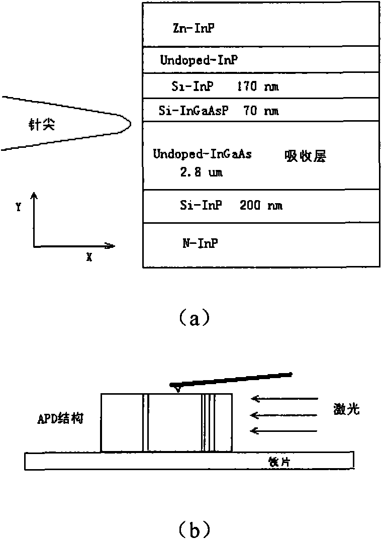
[0021] Taking InGaAs / InP avalanche diode (APD) as an example below, the specific implementation of the present invention will be described in detail in conjunction with the accompanying drawings:

[0022] The tested device is an InGaAs / InP avalanche diode structure grown by metal organic chemical vapor deposition (MOCVD), see figure 1 (a). On the n-type InP substrate are n-type InP layer, unintentionally doped InGaAs absorption layer, n-type InGaAsP layer, n-type InP layer, unintentionally doped InP multiplication layer and p-type InP layer. Here, we define the device growth direction as the Y direction, and the direction perpendicular to the device growth direction as the X direction. After the device is cleaved along the Y direction, stick it on a small iron sheet with conductive silver glue, and the cleavage surface in the Y direction to be tested is vertically upward, opposite to the pasting surface (see figure 1 (b)).

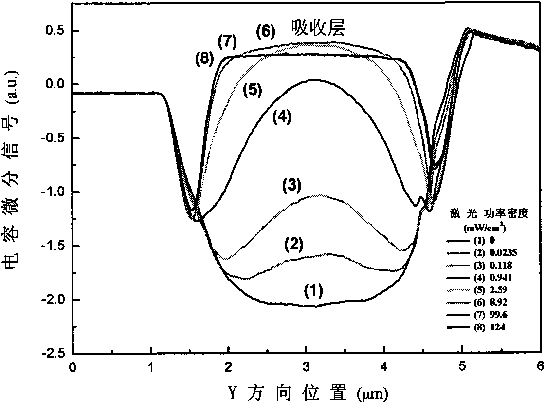
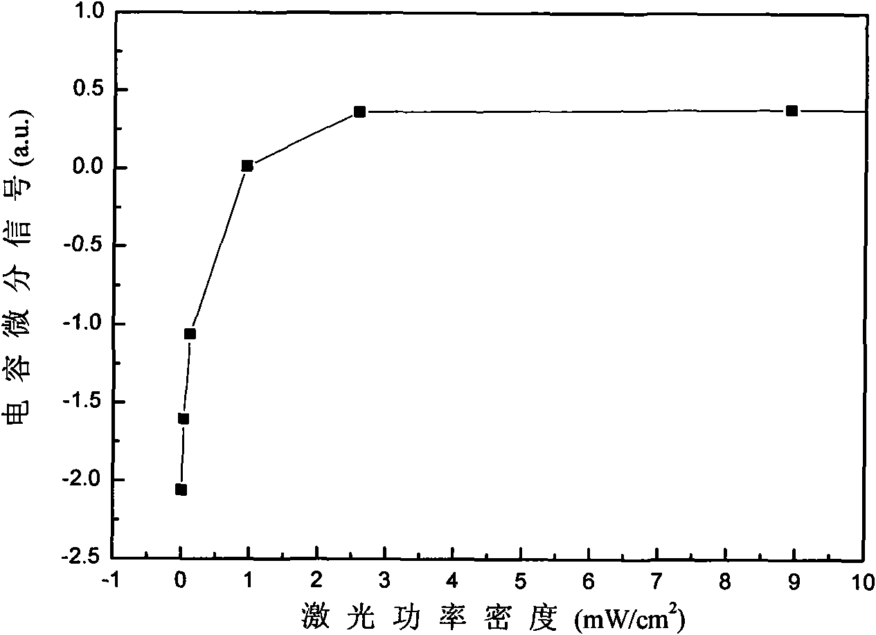
[0023] The measurement of capacitance differentia...


PUM


Abstract

The invention discloses a method for detecting surface leakage channel of semiconductor detection device under illumination. The method judges the existence of surface leakage, that is, surface reflective layer, caused by illumination by measuring capactive differential signal on surface of device in different illumination intensities. By combining the measuring data, the size of the specific leakage channel of the measuring region is obtained through corresponding numerical value simulation. By using this method, the specific surface leakage characteristic of the device is directly and definitely obtained so as to provide parameters having direction for the suppression of the device leakage. The invention has significance on improving the device performance and optimizing the device design.

Description

Technical field: [0001] The invention relates to the measurement of the performance of a semiconductor photodetection device, in particular to a method for measuring a leakage channel generated on the surface of a semiconductor photodetection device under illumination. Background technique: [0002] Among the factors affecting the performance of photodetectors, the leakage characteristic is a crucial parameter, which can affect the noise level and sensitivity of the detector. Studying how to improve the leakage characteristics of the device is an important topic to optimize the performance of the device, and it is a very concerned issue in the current detector technology. There are many factors that cause device leakage, and among them, the surface properties of the sides perpendicular to the growth direction will affect the leakage characteristics of the device. For example, under the action of the surface potential, the surface will appear inversion. The inversion region...

Claims


Application Information

Patent Timeline
IPC IPC(8): G01M11/00G01R31/00
Inventor 陆卫殷豪李天信胡伟达王文娟甄红楼李宁陈平平李志锋陈效双李永富龚海梅
Owner SHANGHAI INST OF TECHNICAL PHYSICS - CHINESE ACAD OF SCI
Why Eureka
Try Eureka