Process for manufacturing semiconductor device and semiconductor device manufactured by such process

A semiconductor and device technology, which is applied to the process of manufacturing semiconductor devices and the field of semiconductor devices manufactured by this process, can solve problems such as preventing voids, and achieve the effect of preventing quality degradation

Inactive Publication Date: 2009-10-07
RENESAS ELECTRONICS CORP
View PDF3 Cites 0 Cited by
  • Summary
  • Abstract
  • Description
  • Claims
  • Application Information

AI Technical Summary

Problems solved by technology

Therefore, it is difficult to firmly prevent the generation of voids in the underfill

Method used


Image

  • Process for manufacturing semiconductor device and semiconductor device manufactured by such process
  • Process for manufacturing semiconductor device and semiconductor device manufactured by such process
  • Process for manufacturing semiconductor device and semiconductor device manufactured by such process

Examples


example 1

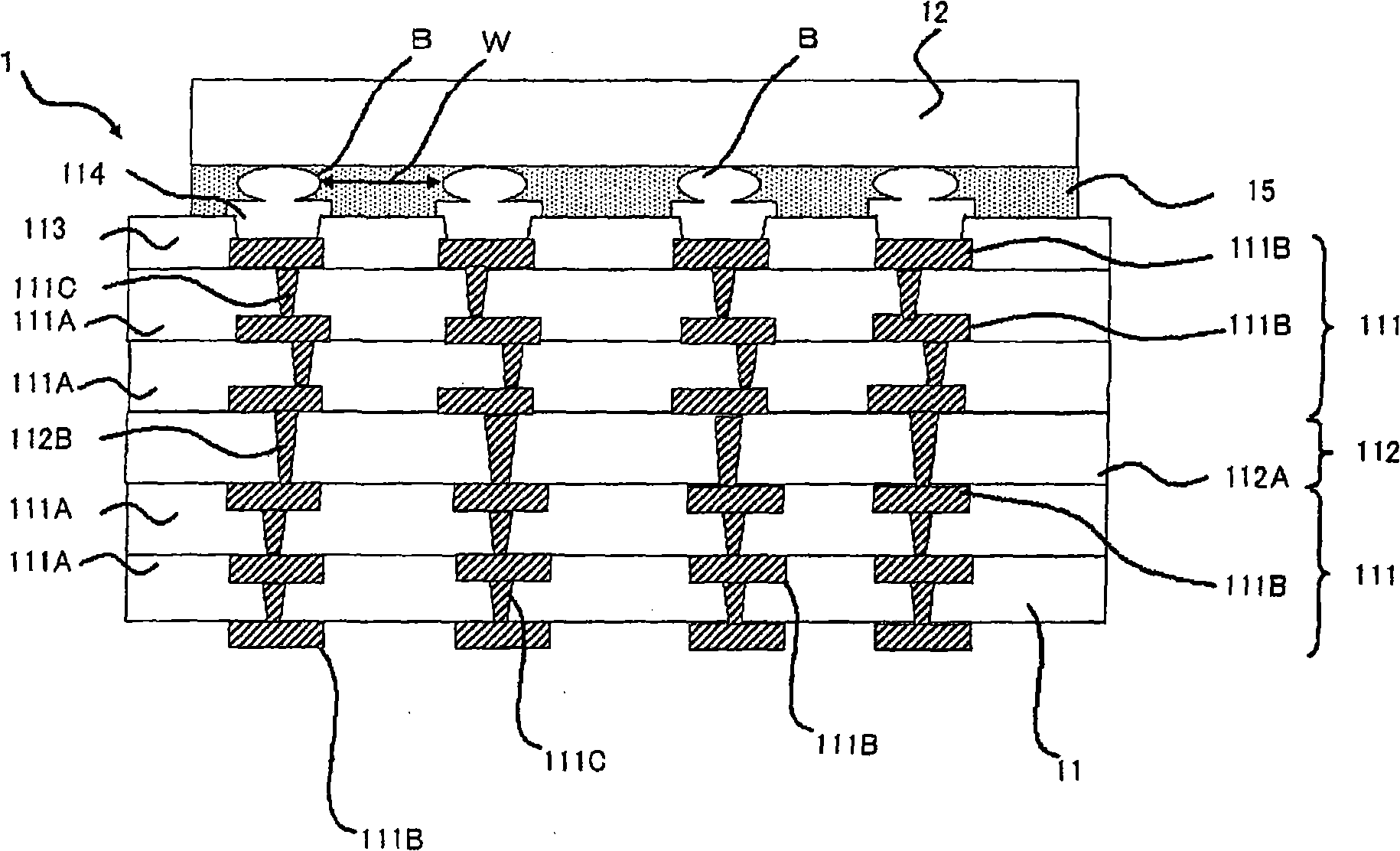
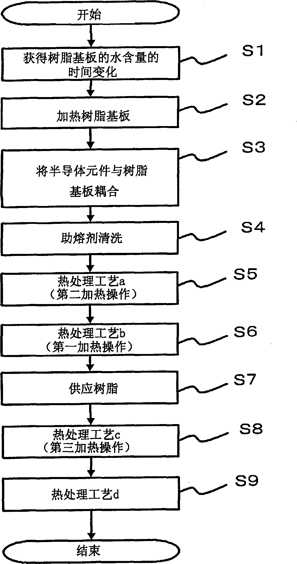
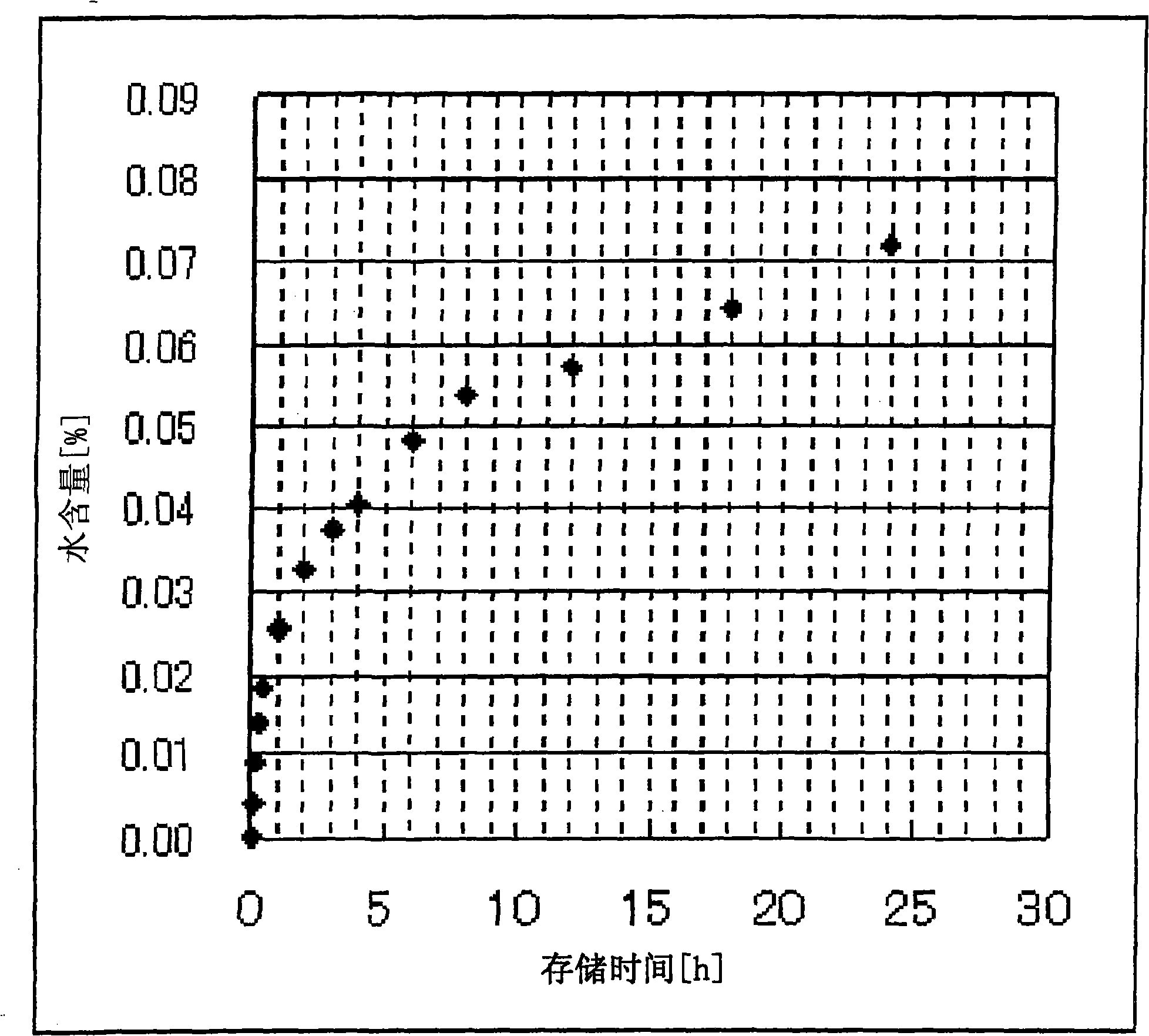
[0063] Next, similarly to the above-described embodiment, a semiconductor element is mounted on the resin substrate, and processing S2 to processing S5 are performed. The bump pitch (inter-bump distance) of the bumps for coupling the semiconductor element and the resin substrate was 169 μm. The solder portion of the resin substrate and the above-mentioned bumps are made of lead-free solder (more specifically, Sn 3 Ag 0.5 Cu) composition. Thereafter, the substrate was left in the clean room for 480 minutes at a temperature of 22.5° C. and a humidity of 50%. according to image 3 and 4 , the water content of the substrate at this time was considered to be 0.055%. Next, the semiconductor device was set in a heating device (the periphery of the heating unit (hot plate) was opened to atmospheric air) at a temperature of 95° C., and then taken out after 150 seconds. In this case, the water content of the resin substrate was 0.02% ( Figure 5 ). The resin was supplied (underf...

example 2

[0065] Similar to Example 1, a semiconductor device having a resin substrate having a water content of 0.055% was installed in a heating device, and taken out after 330 seconds. At this time, the water content of the substrate was 0.017%. The resin was supplied within 3 minutes after the substrate was taken out from the heating apparatus. Since the supply of the resin was started within 3 minutes, the water content of the resin substrate was considered to be 0.017%. Then, the resin was cured similarly to Example 1.


PUM


Abstract

A process for manufacturing a semiconductor device and a semiconductor device manufactured on such manufacturing process are presented. An operation of determining time-variation of water content in the resin substrate 11 (processing S1); an operation of coupling the semiconductor element 12 onto the resin substrate 11 through a plurality of electroconductive bumps B (processing S3); a first heating operation for controlling a water content of the resin substrate 11 to equal to or lower than 0.02% by heating said resin substrate and said semiconductor element while maintaining the coupling through said bumps (processing S6); and a first heating operation for controlling a water content of the resin substrate 11 to equal to or lower than 0.02% by heating said resin substrate and said semiconductor element while maintaining the coupling through said bumps (processing S6); and filling spaces formed by the semiconductor element 12, the resin substrate 11 and the solder bumps B with the resin 15, under the condition that the water content in the resin substrate 11 is equal to or lower than 0.02% (processing S7); are conducted.

Description

[0001] This application is based on Japanese Patent Application No. 2008-096912, the contents of which are incorporated herein by reference. technical field [0002] The present invention relates to a process for manufacturing a semiconductor device and a semiconductor device manufactured by the process. Background technique [0003] In general, a flip chip structure is a suitable packaging technique for semiconductor elements having more than thousands of pins. In this structure, the semiconductor element is coupled to the substrate via bumps. In order to provide protection to the bumps, a resin called underfill is injected into gaps formed among the substrate, semiconductor elements, and bumps, and the injected resin is cured. [0004] In this structure, when underfill is utilized, the following problems are known. When a large amount of water is contained in the substrate during curing of the underfill resin, the water evaporates from the substrate, creating voids in th...

Claims


Application Information

Patent Timeline
Patent Type & Authority Applications(China)
IPC IPC(8): H01L21/60H01L21/48H01L21/56H01L21/66
CPCH01L2224/73203H01L23/145H01L21/563H01L2924/01078H01L24/81H01L2224/73204H01L2224/16225H01L2224/8121H01L2224/81815H01L2224/81801H01L2224/16H01L2224/32225H01L2924/00
Inventor 猪俣辉司
Owner RENESAS ELECTRONICS CORP
Why Eureka
Try Eureka