Color-adjustable organic electroluminescent device and preparation method thereof
A technology of luminescence and organic electronics, which is applied in the field of color-tunable organic electroluminescent devices and their preparation, can solve the problems of reducing device current density, device luminous efficiency attenuation, and high operating voltage, so as to improve recombination probability and efficiency, improve The effect of transmission ability and delay attenuation
- Summary
- Abstract
- Description
- Claims
- Application Information
AI Technical Summary
Problems solved by technology
Method used
Image

Examples
Embodiment 1
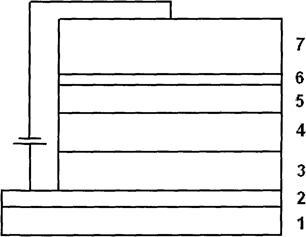
[0038] Firstly, the ITO anode layer on the ITO glass is chemically etched into strip electrodes with a width of 10 mm and a length of 30 mm, and then ultrasonically cleaned with cleaning solution and deionized water for 15 minutes and dried in an oven. Then put the dried substrate into the pretreatment vacuum chamber, and then transfer the ITO anode to the organic evaporation chamber after 10 minutes of low-pressure oxygen plasma treatment with a voltage of 400 volts in an atmosphere of 10 Pa. In a vacuum of 1-5 x 10 -5 In Pa's organic evaporation chamber, a 50-nm-thick AlQ-doped NPB hole-transport layer / luminescent layer, a 30-nm-thick BCP hole-blocking layer, and a 30-nm-thick AlQ electron-transport layer were sequentially evaporated on the ITO layer . Next, the unfinished devices are transferred to a metal evaporation chamber at 5-8 x 10 -5 A 1.0-nm-thick LiF buffer layer was evaporated under a vacuum atmosphere of Pascal, and finally a 100-nm-thick metal Al electrode was...
Embodiment 2
[0040] Firstly, the ITO anode layer on the ITO glass is chemically etched into strip electrodes with a width of 10 mm and a length of 30 mm, and then ultrasonically cleaned with cleaning solution and deionized water for 15 minutes and dried in an oven. Then put the dried substrate into the pretreatment vacuum chamber, and then transfer the ITO anode to the organic evaporation chamber after 10 minutes of low-pressure oxygen plasma treatment with a voltage of 400 volts in an atmosphere of 10 Pa. In a vacuum of 1-5 x 10 -5 In Pa's organic evaporation chamber, a 40-nm-thick AlQ-doped NPB hole-transport layer / luminescent layer, a 30-nm-thick BCP hole-blocking layer, and a 30-nm-thick AlQ electron-transport layer were sequentially evaporated on the ITO layer. . Next, the unfinished devices are transferred to a metal evaporation chamber at 5-8 x 10 -5 A 1.0 nm-thick LiF buffer layer was evaporated under a vacuum atmosphere of Pascal, and finally a 100 nm-thick metal Al electrode wa...
Embodiment 3
[0042] Firstly, the ITO anode layer on the ITO glass is chemically etched into strip electrodes with a width of 10 mm and a length of 30 mm, and then ultrasonically cleaned with cleaning solution and deionized water for 15 minutes and dried in an oven. Then put the dried substrate into the pretreatment vacuum chamber, and then transfer the ITO anode to the organic evaporation chamber after 10 minutes of low-pressure oxygen plasma treatment with a voltage of 400 volts in an atmosphere of 10 Pa. In a vacuum of 1-5 x 10 -5 In Pa's organic evaporation chamber, a 50-nm-thick AlQ-doped NPB hole-transport layer / luminescent layer, a 30-nm-thick BCP hole-blocking layer, and a 30-nm-thick AlQ electron-transport layer were sequentially evaporated on the ITO layer . Next, the unfinished devices are transferred to a metal evaporation chamber at 5-8 x 10 -5 A 1.0 nm-thick LiF buffer layer was evaporated under a vacuum atmosphere of Pascal, and finally a 100 nm-thick metal Al electrode was...
PUM
| Property | Measurement | Unit |
|---|---|---|
| area | aaaaa | aaaaa |
| thickness | aaaaa | aaaaa |
| thickness | aaaaa | aaaaa |
Abstract
Description
Claims
Application Information