Capacitance touch screen and preparation method thereof
The technology of a capacitive touch screen and a manufacturing method, which are applied in electrical digital data processing, ion implantation plating, coating and other directions, can solve the problems of low light transmittance and large thickness, and achieve enhanced light transmittance and thin thickness. , the effect of thickness reduction
- Summary
- Abstract
- Description
- Claims
- Application Information
AI Technical Summary
Problems solved by technology
Method used
Image

Examples
Embodiment 1
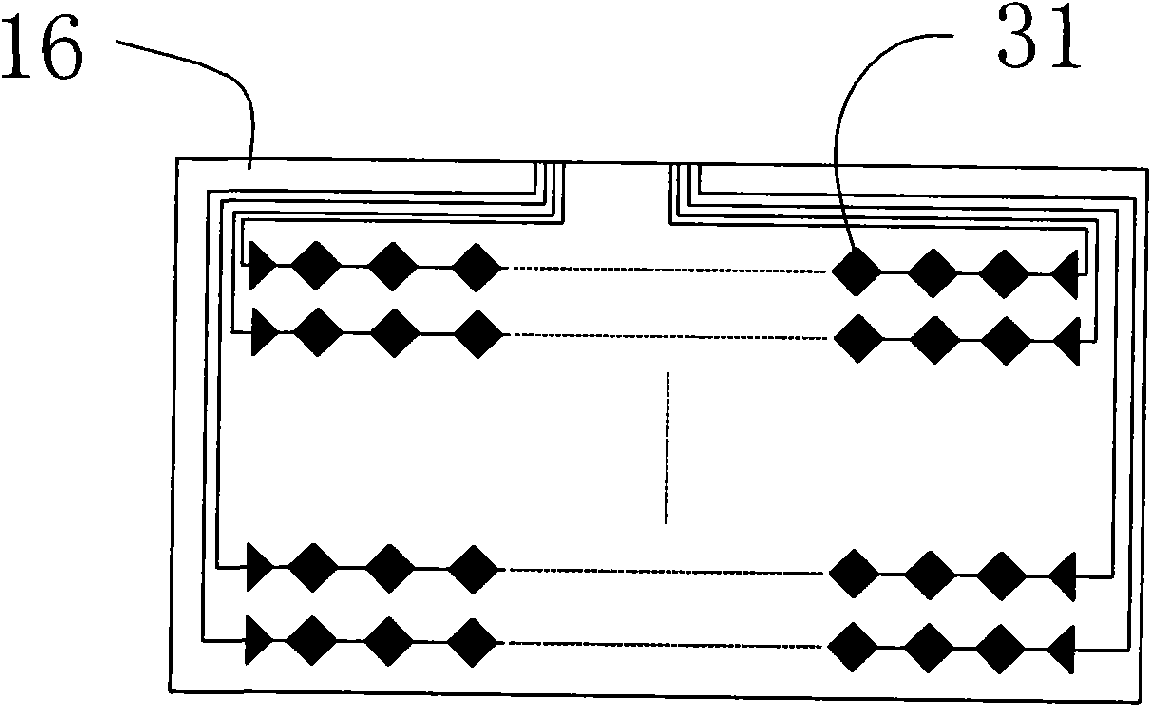
[0040] In the first embodiment of the present invention, the first layer of electrode layer ITO, that is, indium tin oxide (the same below), is sputtered on one side of the substrate 16, and the required ITO pattern 31 is etched out, such as image 3 As shown, then the upper insulating layer 14 is sputtered, and then the second layer of ITO is sputtered, and the required ITO pattern 32 is etched out, as Figure 4 As shown, a layer of transparent liquid insulating layer is prepared by known methods such as offset printing and screen printing, and after the liquid insulating layer is solidified, the transparent insulating layer 18 is formed to obtain the required touch screen. Such as Figure 5 shown.
[0041] The main component of the aforementioned material for preparing the transparent insulating layer 18 is SiO 2 Specifically, you can choose to choose the manufacturer as: Nissan Chemical Industries Co., Ltd. (English name: NISSAN chemical industries, Ltd.), the specific mo...
Embodiment 3
[0048] In the third embodiment of the present invention, the first layer of ITO is sputtered on one side of the substrate, and the required ITO pattern 31 is etched out, such as Figure 11 shown, or Figure 12 As shown, a layer of transparent liquid insulating layer is prepared by offset printing or screen printing, and after the liquid insulating layer is solidified, the transparent insulating layer 18 is formed to obtain the required touch screen. Such as Figure 13 shown.
Embodiment 4
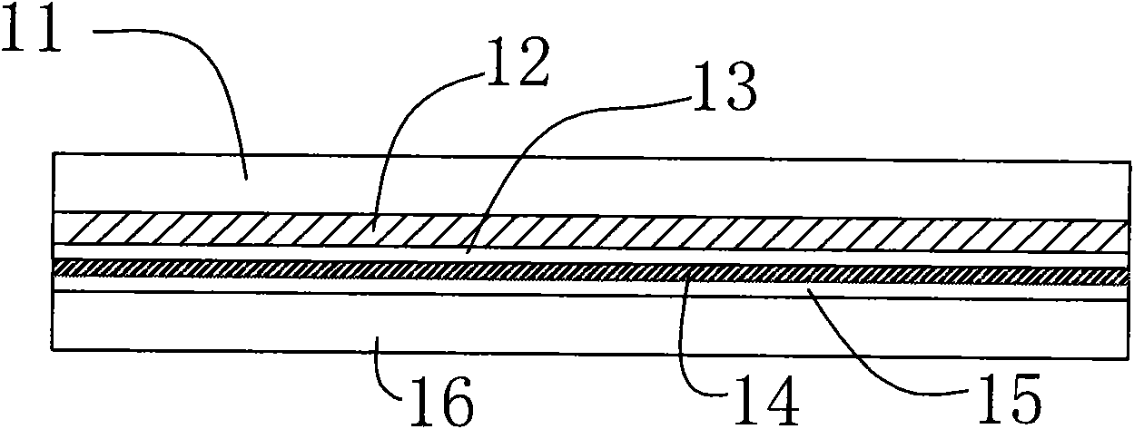
[0050] In the fourth embodiment of the present invention, the first layer of ITO is sputtered on one side of the substrate, and the required ITO pattern 31 is etched out, such as image 3 As shown, then the upper insulating layer is sputtered, and then the second layer of ITO (indium tin oxide) is sputtered, and the required ITO pattern 32 is etched out, such as Figure 4 As shown, sputter a layer of metal electrodes (such as chromium or aluminum or molybdenum, etc.), and etch a metal wiring pattern 35 around it, such as Figure 14 As shown, a layer of transparent liquid insulating layer is prepared by offset printing or screen printing, and after the liquid insulating layer is solidified, the transparent insulating layer 18 is formed, so as to obtain the required touch screen, such as Figure 15 As shown, 35 is the metal wiring, 13 is the second ITO electrode layer, 15 is the first ITO electrode layer, 14 is the insulating layer between the two ITO layers, and 16 is the subst...
PUM
 Abstract
Description
Claims
Application Information
 - R&D Engineer
- R&D Manager
- IP Professional
- Industry Leading Data Capabilities
- Powerful AI technology
- Patent DNA Extraction
Browse by: Latest US Patents, China's latest patents, Technical Efficacy Thesaurus, Application Domain, Technology Topic.
© 2024 PatSnap. All rights reserved.Legal|Privacy policy|Modern Slavery Act Transparency Statement|Sitemap