Wafer socket and method for detecting horizontal positioning of wafer

A technology for horizontal positioning and chip application in measuring devices, surveying and navigation, measuring inclination, etc., which can solve problems such as damage to the chip 22, inaccurate positioning of the chip in the chip socket, and inability to obtain test results, etc., to achieve the effect of avoiding damage

Inactive Publication Date: 2009-11-11
KING YUAN ELECTRONICS
View PDF2 Cites 7 Cited by
  • Summary
  • Abstract
  • Description
  • Claims
  • Application Information

AI Technical Summary

Problems solved by technology

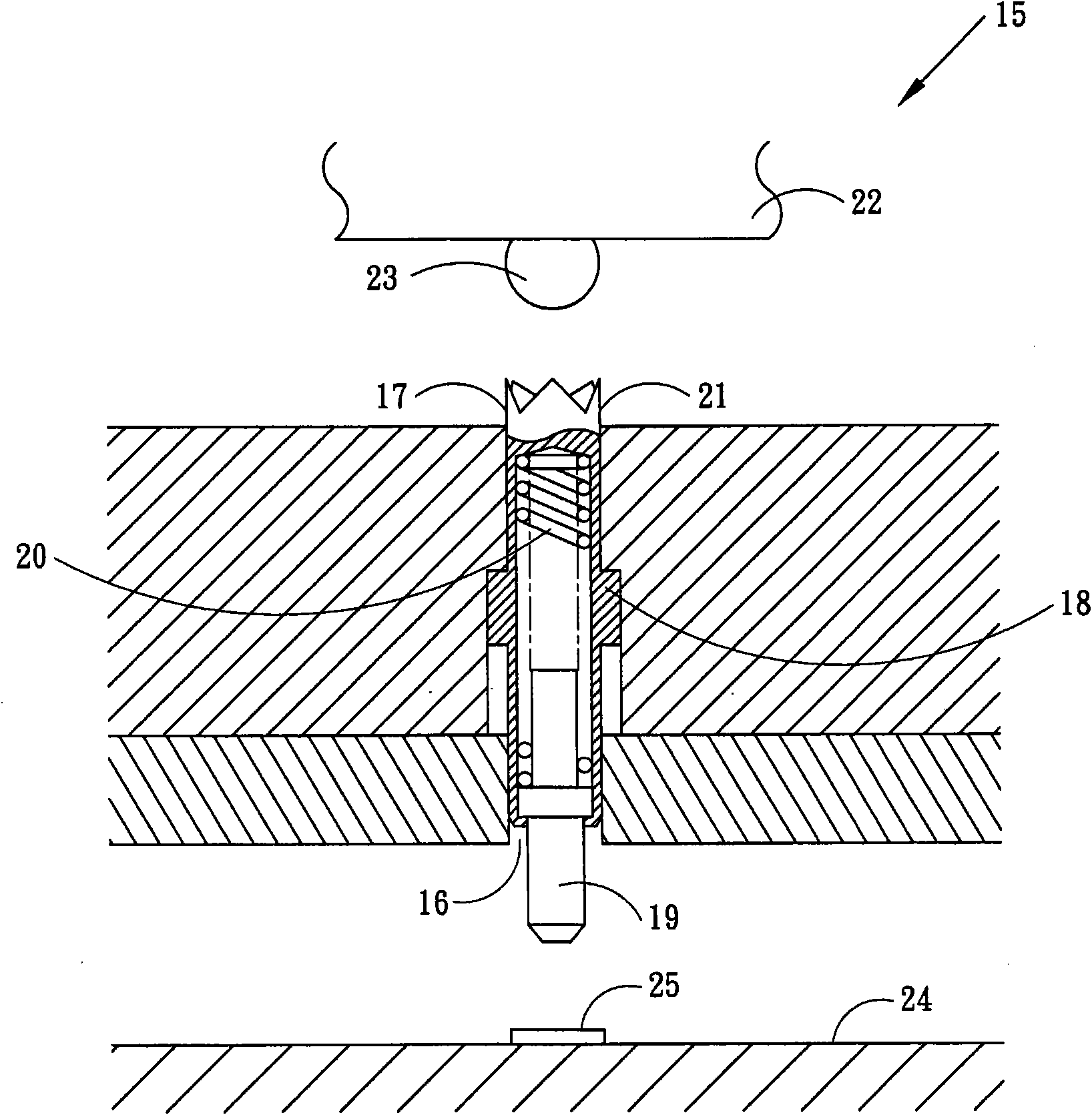
When the size of the chip is smaller, it is more difficult to place the chip accurately, but unfortunately, when the size of the chip is smaller, the allowable positioning deviation is also smaller, and the allowable deviation may be only 0.1mm or even more Small
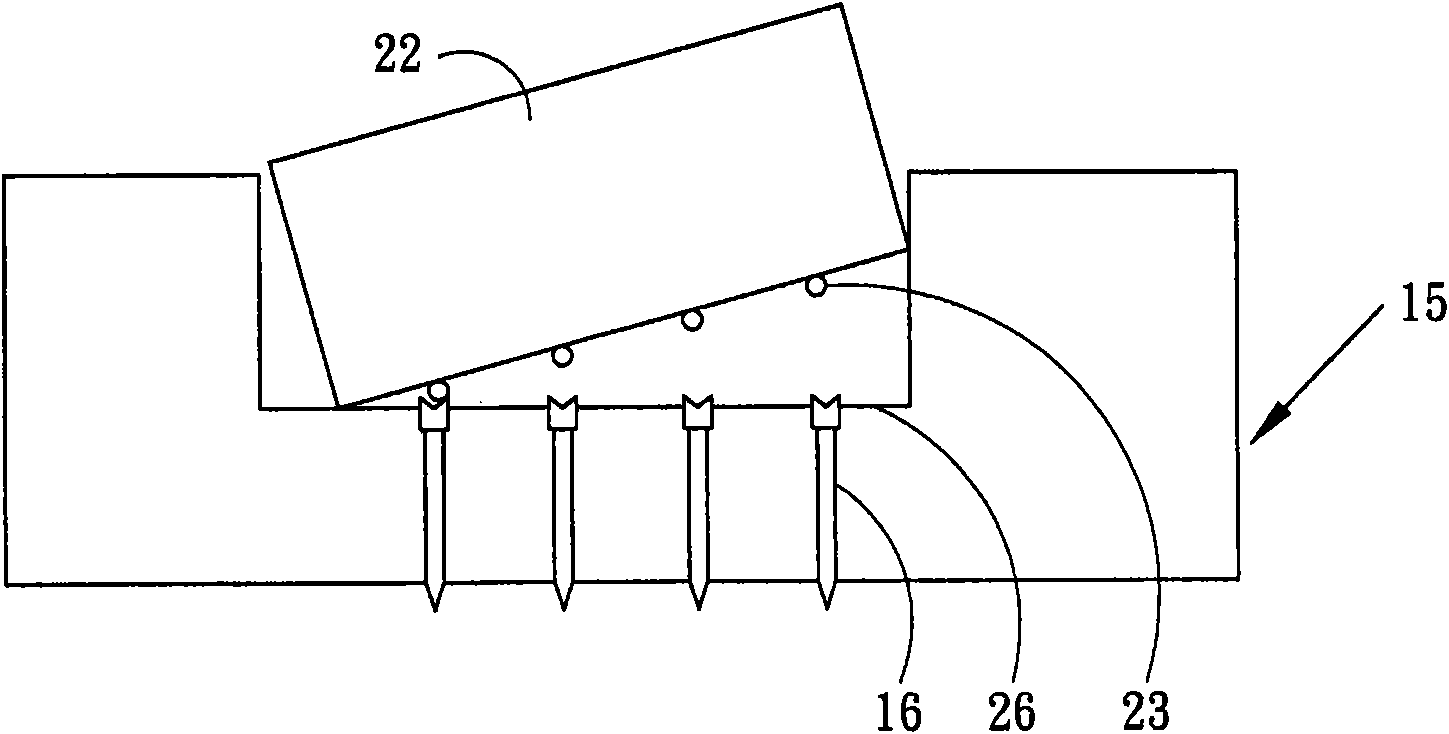
[0007] figure 2 Situation showing that the chip of the existing known chip socket cannot be accurately positioned
Wafer socket 15 has a horizontal positioning surface 26, and the cross-sectional area of ​​positioning surface 26 is slightly larger than the cross-sectional area of ​​the wafer. For some reasons, such as the wafer size is too small and the weight is too light, the wafer 22 exceeds the allowable offset when placed. , resulting in the chip 22 not being placed horizontally in the positioning surface 26, so that the solder ball 23 of the chip is not connected to the probe 16, so that the correct test result cannot be obtained
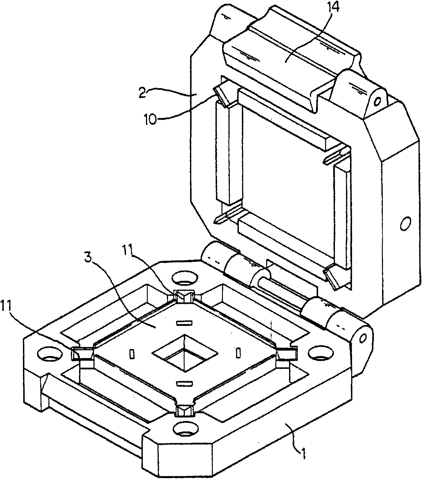
[0008] Also, if wafer sockets are such as figure 1 With the structure of the upper cover 2, when the wafer 22 cannot be accurately positioned horizontally, the wafer 22 will be damaged when the upper cover 2 is pressed down, which increases the manufacturing cost
[0009] This shows that above-mentioned existing wafer socket obviously still has inconvenience and defect in structure, method and use, and urgently needs to be further improved
In order to solve the above-mentioned problems, the relevant manufacturers have tried their best to find a solution, but for a long time no suitable design has been developed, and the general product has no suitable structure to solve the above-mentioned problems. This is obviously the relevant industry. Urgent problem

Method used


Image

  • Wafer socket and method for detecting horizontal positioning of wafer
  • Wafer socket and method for detecting horizontal positioning of wafer
  • Wafer socket and method for detecting horizontal positioning of wafer

Examples


Embodiment Construction

[0063] For further elaborating the technical means and effects that the present invention adopts for reaching the intended invention purpose, below in conjunction with accompanying drawing and preferred embodiment, to its specific implementation mode, structure of the wafer socket proposed according to the present invention and the method for detecting the horizontal orientation of wafer , method features and effects thereof are described in detail below.

[0064] The aforementioned and other technical contents, features and effects of the present invention will be clearly presented in the following detailed description of preferred embodiments with reference to the drawings. For convenience of description, in the following embodiments, the same elements are denoted by the same numbers.

[0065] Figure 4 A wafer socket of an embodiment of the invention is shown. The wafer socket 30 includes a base 32 . The base 32 includes a positioning surface 33 for accommodating a wafer ...


PUM


Abstract

The invention relates to a wafer socket and a method for detecting horizontal positioning of wafer. The wafer socket comprises a base and an assembly, wherein the base is provided with a positioning surface for accommodating the wafer and two pairs of optical inductors are respectively arranged in the assembly and are close to regions of two diagonal lines so as to detect whether the wafer is horizontally positioned. The invention aims at ensuring that the wafer is placed at the right place so as to prevent the wafer from being damaged during the test and ensure that the test can be smoothly performed.

Description

technical field [0001] The invention relates to a wafer socket, in particular to a wafer socket capable of detecting whether the wafer is positioned horizontally. Background technique [0002] The function of the IC socket is to electrically connect a plurality of protruding terminals (pins or leads) of the chip to a plurality of soldering pads (pads) of the circuit board for testing. Chip sockets are consumables, and can also be replaced according to the type of test chip. Therefore, a well-designed chip socket must be easy to replace. [0003] In addition to easy replacement, whether the chip is placed in the correct position is also an important issue. Such as figure 1 As shown, US Pat. No. 5,100,332 discloses a wafer socket comprising a base 1 and an upper cover 2 . The base 1 has a bearing surface 3 with grooves for accommodating wafers to be tested (not shown); The wafer socket is characterized in that the four corners of the base 1 have a V-shaped recessed structu...

Claims


Application Information

Patent Timeline
Patent Type & Authority Applications(China)
IPC IPC(8): H01R33/74H01R13/629H01R13/24G01R1/04G01C9/00
Inventor 温进光
Owner KING YUAN ELECTRONICS
Why Eureka
Try Eureka