Microchip and process for producing microchip
A manufacturing method and microchip technology, applied in chemical instruments and methods, manufacturing microstructure devices, microelectronic microstructure devices, etc., can solve problems such as high cost and glass substrates are not suitable for mass production, and achieve the effect of preventing leakage
- Summary
- Abstract
- Description
- Claims
- Application Information
AI Technical Summary
Problems solved by technology
Method used
Image

Examples
no. 1 approach
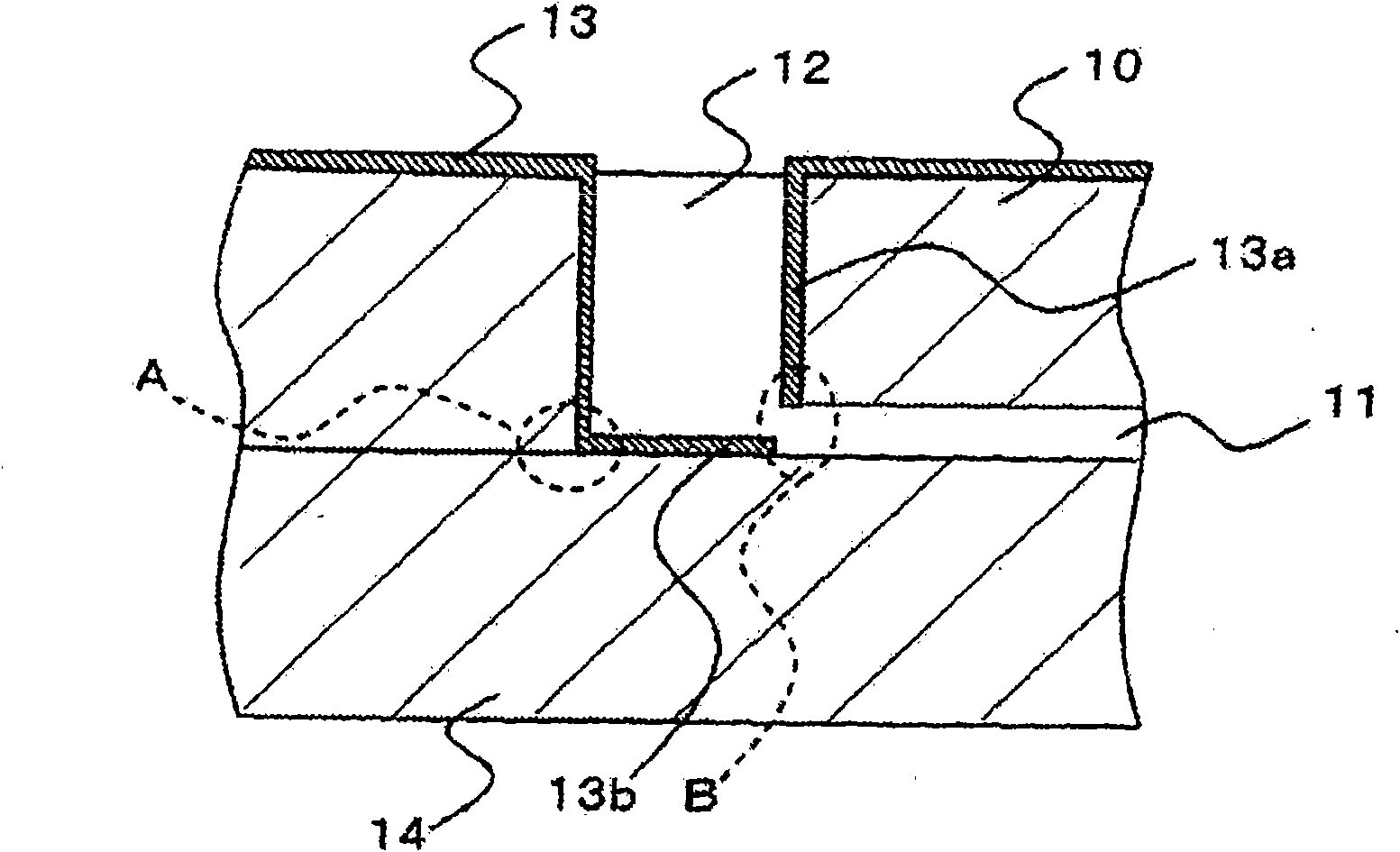
[0043] refer to figure 1 A microchip according to a first embodiment of the present invention and a method of manufacturing the microchip will be described. figure 1 is a cross-sectional view of the microchip according to the first embodiment of the present invention.
[0044] (Structure of Microchip)
[0045] The microchip according to the first embodiment is configured to have a microchip substrate 10 and a microchip substrate 14 . Groove-shaped fine flow paths 11 are formed on the microchip substrate 10 . Further, a through-hole penetrating the substrate is formed in the microchip substrate 10 . The through hole is formed in contact with the fine flow path 11 , and becomes the opening 12 by joining the microchip substrate 10 and the microchip substrate 14 . The microchip substrate 14 to be bonded to the microchip substrate 10 is a planar substrate. The microchip substrate 10 and the microchip substrate 14 are bonded with the surface on which the fine channel 11 is form...
no. 2 approach
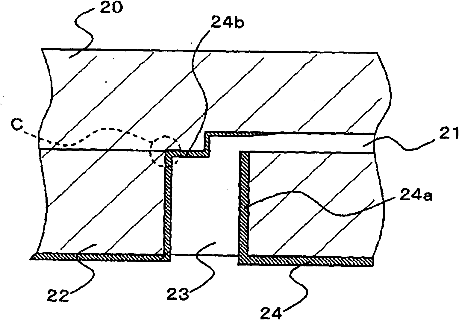
[0099] Next, refer to figure 2 A microchip and a method of manufacturing the microchip according to the second embodiment of the present invention will be described. figure 2 is a cross-sectional view of a microchip according to a second embodiment of the present invention. A through-hole is formed in the microchip substrate serving as the lid in the second embodiment.
[0100] The microchip according to the second embodiment is configured to have a microchip substrate 20 and a microchip substrate 22 . Groove-shaped fine flow paths 21 are formed on the microchip substrate 20 . The microchip substrate 22 to be bonded to the microchip substrate 20 is a planar substrate. In the second embodiment, through-holes are formed in the microchip substrate 22 . The microchip substrate 20 and the microchip substrate 22 are bonded with the surface on which the fine channel 21 is formed as the inner side. Thus, the microchip substrate 22 is used as a cover for the fine channel 21 , an...
no. 3 approach
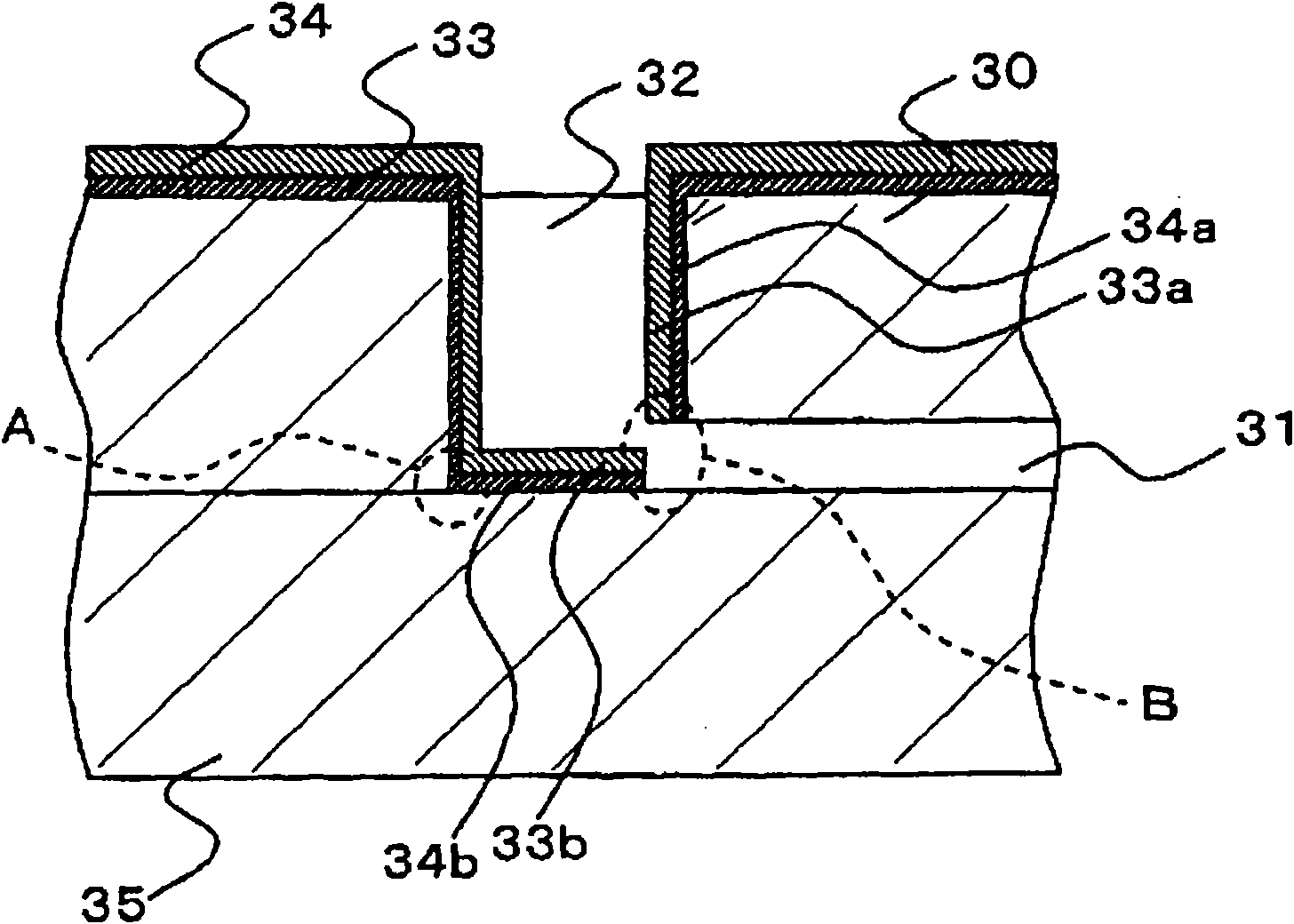
[0108] Next, refer to image 3 A microchip and a method of manufacturing the microchip according to a third embodiment of the present invention will be described. image 3 is a cross-sectional view of a microchip according to a third embodiment of the present invention. In the third embodiment, through-holes are formed in a microchip substrate in which fine flow paths are formed, and two layers of dielectric films are formed in openings.
[0109] (Structure of Microchip)
[0110] The microchip according to the third embodiment is configured to have a microchip substrate 30 and a microchip substrate 35 . Groove-shaped fine flow paths 31 are formed on the microchip substrate 30 . Further, a through hole penetrating the substrate is formed in the microchip substrate 30 . The through hole is formed in contact with the fine flow path 31 , and the opening 32 is formed by joining the microchip substrate 30 and the microchip substrate 35 . The microchip substrate 35 to be bonded ...
PUM
 Abstract
Description
Claims
Application Information
 - R&D
- Intellectual Property
- Life Sciences
- Materials
- Tech Scout
- Unparalleled Data Quality
- Higher Quality Content
- 60% Fewer Hallucinations
Browse by: Latest US Patents, China's latest patents, Technical Efficacy Thesaurus, Application Domain, Technology Topic, Popular Technical Reports.
© 2025 PatSnap. All rights reserved.Legal|Privacy policy|Modern Slavery Act Transparency Statement|Sitemap|About US| Contact US: help@patsnap.com