Supercharge Your Innovation With Domain-Expert AI Agents!

Display panel and pixel defect check method thereof

A technology for display panels and inspection methods, applied in optical testing flaws/defects, static indicators, optics, etc., can solve problems such as high error rate, easy to find wrong positions, and reduced area range

Inactive Publication Date: 2012-05-23
AU OPTRONICS (SUZHOU) CORP LTD +1
View PDF4 Cites 0 Cited by
  • Summary
  • Abstract
  • Description
  • Claims
  • Application Information

AI Technical Summary

Problems solved by technology

Therefore, when looking for defective pixels in the circled area under the optical microscope, it is quite easy for the staff to find the wrong position or it is difficult to quickly find out the abnormal factors among the dozens of circled pixels
Especially when the optical microscope is set to a high magnification, the scope of the area that the microscope can display is greatly reduced, and it is even more difficult for the staff to find defective pixels
Therefore, the defect analysis of the traditional display panel 108 has a high error rate and low efficiency

Method used


Image

  • Display panel and pixel defect check method thereof
  • Display panel and pixel defect check method thereof
  • Display panel and pixel defect check method thereof

Examples


Embodiment Construction

[0051] Embodiments of the present invention will be described in detail below in conjunction with the accompanying drawings.

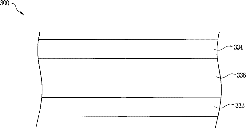
[0052] Please refer to image 3 , is a schematic cross-sectional view of a liquid crystal display panel in a specific embodiment of the present invention. In this specific implementation manner, a liquid crystal display panel is used as the display panel of this embodiment, but the present invention is not limited thereto. The liquid crystal display panel 300 mainly includes an upper substrate 334 , a lower substrate 332 and a liquid crystal layer 336 . The lower substrate 332 is disposed on the opposite side of the upper substrate 334 , and the liquid crystal layer 336 is disposed between the upper substrate 334 and the lower substrate 332 .

[0053] In this embodiment, the upper substrate and the lower substrate 332 of the liquid crystal display panel 300 may be a color filter substrate and a thin film transistor substrate, a color filter substrate a...


PUM


Abstract

The invention discloses a display panel and a pixel defect check method thereof. The display panel comprises a plurality of first pixels and a plurality of second pixels. The second pixels and the first pixels are mixed and arranged into an array. The first pixels and the second pixels have the same opening ratio or / and electric property, and the first pixels and the second pixels have different appearance and structure characteristics.

Description

technical field [0001] The invention relates to an electronic device and a defect inspection method thereof, in particular to a display panel and a pixel defect inspection method thereof. Background technique [0002] Please refer to figure 1 As shown, is a schematic top view of a pixel array of a conventional display panel. The pixel array 100 of the display panel 108 is composed of several pixels 102 arranged in an array. In the pixel array 100 of the conventional display panel 108, each pixel 102 has the same appearance and structural features. [0003] For example, in the pixel array 100 , each pixel 102 includes a storage capacitor 104 . Each storage capacitor 104 includes a via (Via) 106 . Wherein, the storage capacitors 104 are correspondingly arranged in the pixels 102 , and the through holes 106 are correspondingly arranged in the storage capacitors 104 . In the conventional pixel array 100 , the positions of the storage capacitors 104 included in all the pixel...

Claims


Application Information

Patent Timeline
Patent Type & Authority Patents(China)
IPC IPC(8): G02F1/133G02F1/1362G02F1/13G01N21/95
Inventor 王孝林林昆标
Owner AU OPTRONICS (SUZHOU) CORP LTD
Features
  • R&D
  • Intellectual Property
  • Life Sciences
  • Materials
  • Tech Scout
  • Unparalleled Data Quality
  • Higher Quality Content
  • 60% Fewer Hallucinations
Learn More