Circuit board with imbedded electronic device and method of imbedding electronic device therein

A technology for electronic devices and circuit boards, which is applied in the directions of printed circuits connected with non-printed electrical components, assembling printed circuits with electrical components, and manufacturing of multi-layer circuits. Thin circuit boards, etc.

Active Publication Date: 2009-12-02
COMPEQ MFG
View PDF1 Cites 14 Cited by
  • Summary
  • Abstract
  • Description
  • Claims
  • Application Information

AI Technical Summary

Problems solved by technology

However, the height of the vertical electronic device itself, coupled with the vertical electrical connection structure, leads to a substantial increase in the overall thickness of the circuit board, which cannot meet the requ

Method used


Image

  • Circuit board with imbedded electronic device and method of imbedding electronic device therein
  • Circuit board with imbedded electronic device and method of imbedding electronic device therein
  • Circuit board with imbedded electronic device and method of imbedding electronic device therein

Examples


Embodiment Construction

[0029] The method of the present invention is a method for manufacturing a circuit board with embedded electronic devices, and a preferred embodiment thereof is shown in Figure 1-10 , where it is indicated that the method comprises the steps described subsequently.

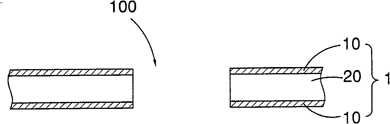
[0030] First, if figure 1 As shown, a core 1 is provided, which includes a dielectric layer 20 and two metal layers 10 covering the upper and lower surfaces of the dielectric layer 20 respectively. The core board 1 defines a through hole 100 in its thickness direction, and the through hole 100 penetrates through the dielectric layer 20 and the metal layer 10 . In this example, the core board 1 is a copper clad substrate (Copper Clad Laminate) whose surface is covered with these metal layers 10, but is not limited thereto. For example, it can be a pre-processed multi-layer circuit board. Combining a dielectric layer with a metal layer. In addition, the through hole 100 can be formed by mechanical or laser dril...


PUM


Abstract

The invention relates to a circuit board with an imbedded electronic device and a method of imbedding the electronic device therein. The circuit board comprises a core board, the electronic device, an insulating filled layer and a conductive structure; the surface of the core board is provided with a line layer and a through hole in which the electronic device is held; two opposite sides of the electronic device are respectively provided with an end electrode which faces to the wall of the through hole of the core board; one end surface of the end electrode is an orifice exposed outside the through hole; the insulating filled layer is filled in a gap formed between the wall of the through hole of the core board and the electronic device; and the conductive structure is in bridge connection with the end surface of the end electrode and the line layer of the core board. The electronic device can be imbedded in the circuit board without causing the thickness increase of the circuit board and has simple manufacture technology.

Description

technical field [0001] The invention relates to the circuit board manufacturing technology, in particular to the technology of embedding and embedding electronic devices in the circuit board. Background technique [0002] With the integration and miniaturization of electronic devices, the requirements for embedding electronic devices in circuit boards are increasing day by day. [0003] US Patent No. 6928726 discloses a circuit board with embedded electronic devices and its manufacturing method. The electrodes at both ends of the electronic device are arranged up and down (vertical), and are "vertically electrically connected" with the upper and lower circuit layers by using blind holes and solder balls. However, the height of the vertical electronic device itself, coupled with the vertical electrical connection structure, leads to a substantial increase in the overall thickness of the circuit board, which cannot meet the requirements of a thin circuit board. [0004] In o...

Claims


Application Information

Patent Timeline
IPC IPC(8): H05K1/18H05K3/30H05K3/46
Inventor 林志谦陈彦瑞李金修
Owner COMPEQ MFG
Why Eureka
Try Eureka