Liquid crystal picture element and producing method thereof and liquid crystal display device

A liquid crystal display, liquid crystal pixel technology, applied in static indicators, semiconductor/solid-state device manufacturing, instruments, etc., can solve problems such as current consumption, and achieve the effect of avoiding parasitic capacitance

Active Publication Date: 2007-08-22
AU OPTRONICS CORP
View PDF0 Cites 14 Cited by
  • Summary
  • Abstract
  • Description
  • Claims
  • Application Information

AI Technical Summary

Problems solved by technology

However, the unnecessary storage capacitance formed by the doped polysilicon layer 200 and the data line 104 also consumes current during the operation of the liquid crystal pixel, thereby causing an additional load burden on the data line 104

Method used


Image

  • Liquid crystal picture element and producing method thereof and liquid crystal display device
  • Liquid crystal picture element and producing method thereof and liquid crystal display device
  • Liquid crystal picture element and producing method thereof and liquid crystal display device

Examples


Embodiment Construction

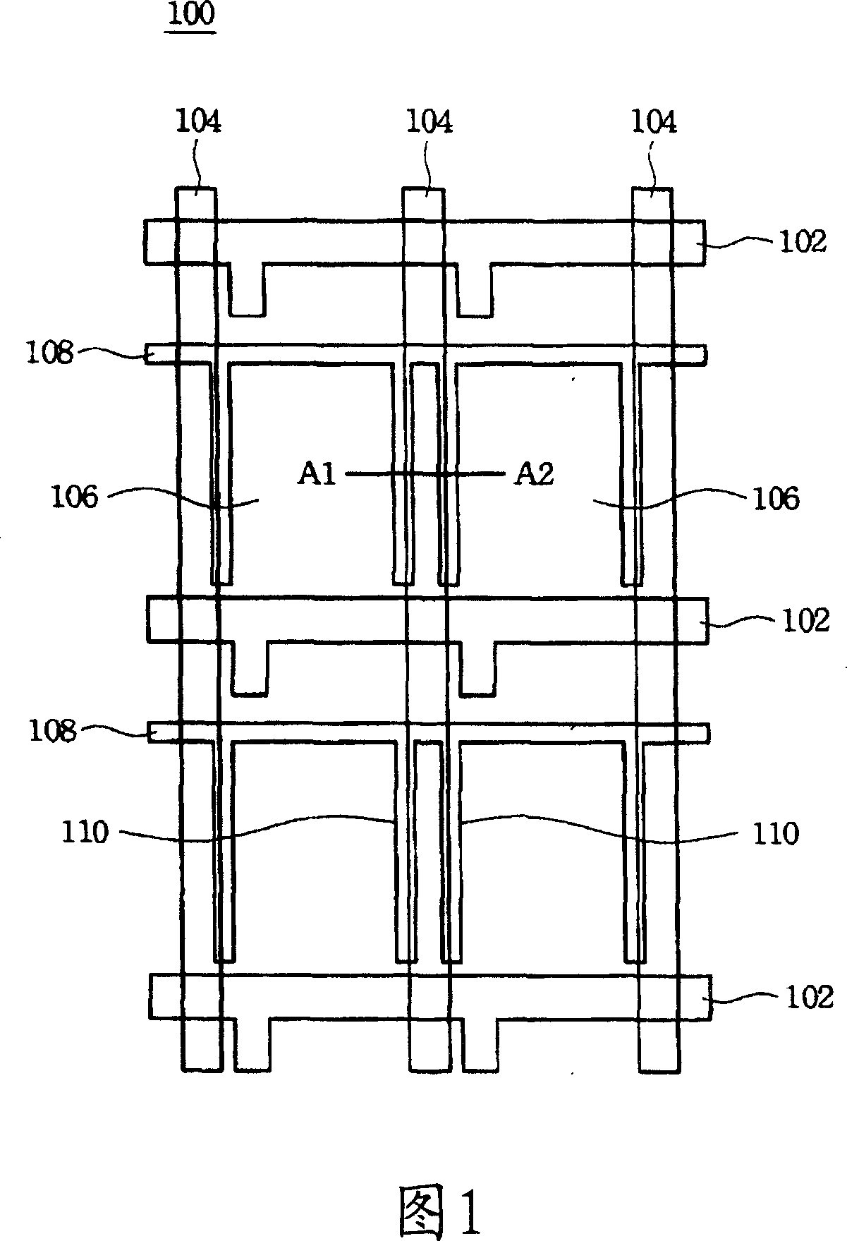
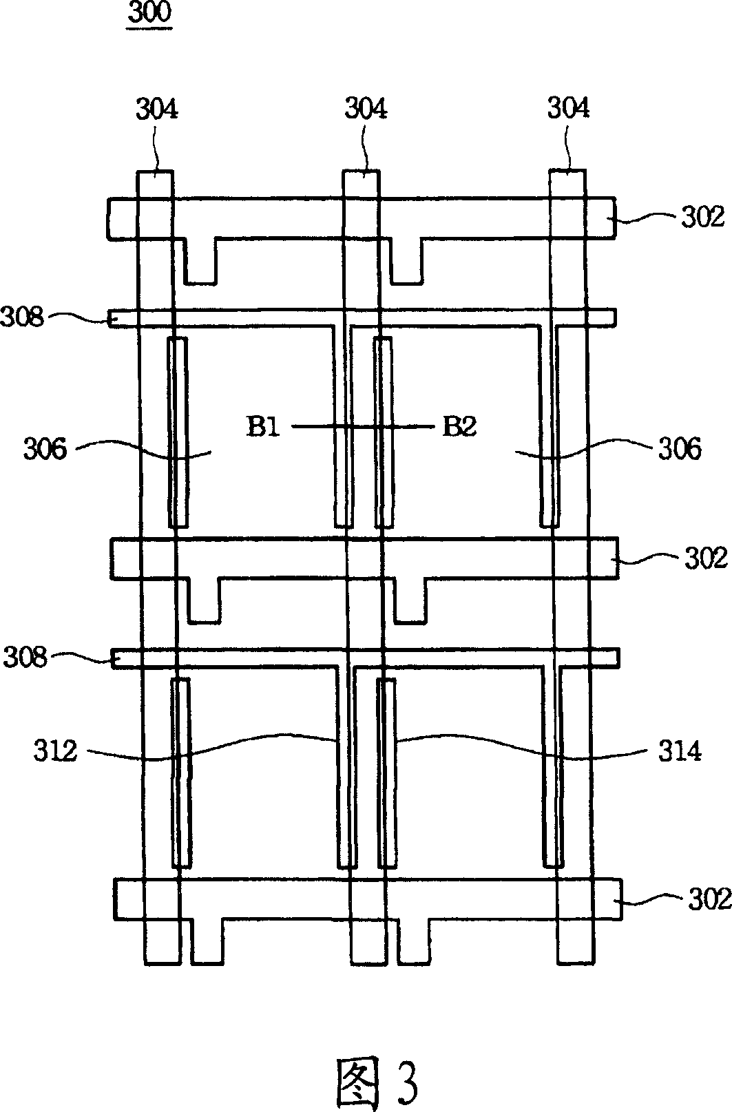
[0027] Please refer to FIG. 3 , which shows a schematic diagram of a display array in a liquid crystal display according to an embodiment of the present invention. The display array 300 includes several scan lines 302 and several data lines 304 , and the scan lines 302 and the data lines 304 intersect to form a plurality of pixel regions 306 . The potential of the common electrode of each row of pixel regions 306 is controlled by a common electrode line 308 . In addition, two sides of each pixel area 306 also include shielding metal layers 312 and 314 , wherein the shielding metal layer 312 is connected to the common electrode line 308 , and the shielding metal layer 314 is not connected to the common electrode line 308 .

[0028] Please refer to FIG. 4 , which shows a cross-sectional view of part B1-B2 in FIG. 3 . The liquid crystal pixel includes data lines 304 , a doped polysilicon layer 412 and a shielding metal layer 312 . The doped polysilicon layer 412 is located belo...


PUM


Abstract

The invention provides a liquid crystal pixel and the making method and LCD thereof. And the liquid crystal pixel comprises a data line, a doped polycrystalline layer and a shielding metal layer, where the doped polycrystalline silicon layer is located under the data line and the vertical projection of the polycrystalline silicon layer does not overlap the data line; the shielding metal layer is located between the data line and the doped polycrystalline silicon layer and form a storage capacitor together with the polycrystalline silicon layer. In addition, the invention also provides a liquid crystal pixel making method, which stores video data by the store capacitor and can not cause burden to the data line but can avoid possible parasitical capacitor between the pixel electrode and the data line.

Description

technical field [0001] The invention relates to the field of liquid crystal pixels, and particularly relates to a liquid crystal pixel capable of reducing the load of data lines in a liquid crystal panel, a manufacturing method thereof and a liquid crystal display. Background technique [0002] In recent years, due to the rapid development of liquid crystal displays and many advantages such as light weight, low power consumption and zero radiation, they are widely used in various electronic products. In a general active matrix liquid crystal display, the liquid crystal pixels are arranged in an array, and the action of each liquid crystal pixel is controlled by an active element such as a thin film transistor. [0003] Please refer to FIG. 1 , which shows a schematic diagram of a display array in a conventional liquid crystal display. The display array 100 includes several scan lines 102 and several data lines 104 , and the scan lines 102 and the data lines 104 intersect to...

Claims


Application Information

Patent Timeline
Patent Type & Authority Applications(China)
IPC IPC(8): G02F1/1362G02F1/133H01L27/12H01L23/522H01L21/84H01L21/768
Inventor 丁友信李雅君尤建盛
Owner AU OPTRONICS CORP
Why Eureka
Try Eureka