
Electron-emitting device, method of manufacturing the same, electron source, and image display apparatus

A technology of electron emission and manufacturing method, applied in the direction of image/graphic display tube, electrode system manufacturing, discharge tube/lamp manufacturing, etc., which can solve the problems of reduced electron emission efficiency and inability to set sufficient gaps, etc., and achieve low power consumption , Prevent leakage current generation, high brightness effect

Inactive Publication Date: 2009-12-30
CANON KK
View PDF1 Cites 0 Cited by
  • Summary
  • Abstract
  • Description
  • Claims
  • Application Information

AI Technical Summary

Problems solved by technology

However, depending on the formation conditions, a sufficient gap cannot be provided between the extended portions of the carbon film pair, so there are cases where end sections (portions away from the conductive film) of the extended portions are connected to each other
[0005] When the extended portions of the carbon film are connected to each other as described above, an ineffective current (leakage current) flows between the device electrodes through the extended portions, and as a result, there is a case where the electron emission efficiency decreases

Method used


Image

  • Electron-emitting device, method of manufacturing the same, electron source, and image display apparatus
  • Electron-emitting device, method of manufacturing the same, electron source, and image display apparatus
  • Electron-emitting device, method of manufacturing the same, electron source, and image display apparatus

Examples


Embodiment Construction

[0026] Hereinafter, a detailed description will be given of preferred embodiments of the present invention for purposes of explanation while referring to the accompanying drawings. Note that dimensions, materials, shapes, relative positions, and the like of components described in the embodiments are not intended to limit the scope of the present invention to the given examples unless specifically mentioned otherwise.

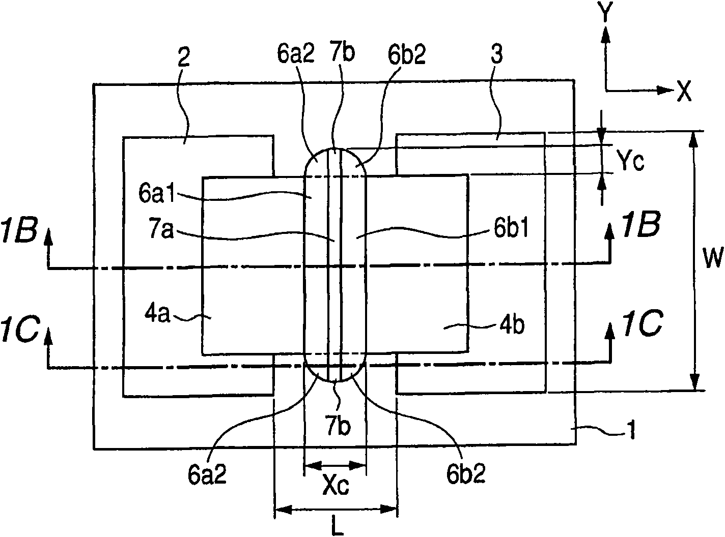
[0027] Figure 1A ~ 1C is a schematic diagram showing an electron-emitting device according to an embodiment of the present invention. Figure 1A is the floor plan. Figure 1B is along Figure 1A Cross-sectional view of line 1B-1B. Figure 1C is along Figure 1A A cross-sectional view of the 1C-1C line.

[0028] Figure 1A ~ 1C A structure in which a first electrode 2 connected to a first conductive film 4 a and a second electrode 3 connected to a second conductive film 4 b are provided on a substrate 1 is shown. However, when the first conductive film 4a a...


PUM


Abstract

The invention provides an electron-emitting device, a method for manufacturing the same, an electron source and an image display apparatus. The electron-emitting device is excellent in electron-emitting efficiency, and may obtain a large electron-emitting amount and stable electron-emitting characteristics. The electron-emitting device includes: a first conductive film and a second conductive film which are provided through a first gap; first carbon films connected to the first conductive film; and second carbon films which are connected to the second conductive film, and are opposed to the first carbon films through second and third gaps. Continuous concave portions are provided in the second and third gaps.

Description

technical field [0001] The present invention relates to an electron emission device for a flat panel display, a method of manufacturing the electron emission device, an electron source including the electron emission device, and an image display device using the electron source. Background technique [0002] Surface conduction electron-emitting devices are based on the phenomenon that a conductive film formed on an insulating substrate is supplied with a current parallel to the surface of the conductive film to emit electrons. Basically, a pair of device electrodes is formed on a substrate. A conductive film is formed to connect device electrodes to each other. A minute gap is provided in the conductive film to form a pair of conductive films. An operation called "activation" is performed to deposit a pair of carbon films in the gap and on a portion of the conductive film close to the gap. The pair of carbon films has a minute gap, and each of the carbon films is connecte...

Claims


Application Information

Patent Timeline
Patent Type & Authority Applications(China)
IPC IPC(8): H01J1/316H01J29/04H01J31/12H01J9/02
CPCH01J31/127H01J2329/0489H01J2201/3165H01J1/316H01J9/027
Inventor 岛津晃
Owner CANON KK
Learn More