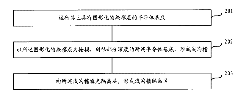
Inorganic film etching method in semiconductor manufacture procedure and shallow groove isolation area forming method
A shallow trench isolation region, inorganic film technology, applied in semiconductor/solid-state device manufacturing, electrical components, circuits, etc., can solve problems such as poor operability, and achieve the effect of enhancing consistency and reducing the possibility of by-products
- Summary
- Abstract
- Description
- Claims
- Application Information
AI Technical Summary
Problems solved by technology
Method used
Image

Examples
no. 1 example
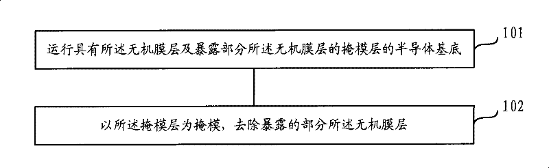
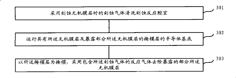
[0044] As a first embodiment of the present invention, the inorganic film layer includes a polysilicon layer; the operation of etching the inorganic film layer may be an operation of etching the polysilicon gate layer to form a polysilicon gate layer after forming the polysilicon gate layer .
[0045] When the inorganic film layer includes a polysilicon layer, the etching gas includes SiCl 4 , the SiCl 4 The flow range is 10-300sccm, such as 30sccm, 90sccm, 120sccm, 150sccm; when performing the cleaning operation, the reaction power is 500-2000W, such as 1000W, 1250W, 1500W; when performing the cleaning operation, the reaction pressure is 10-2000W 100mT, such as 50mT, 65mT, 80mT; when performing the cleaning operation, the duration of the pre-cleaning operation is 5-20 seconds, such as 10 seconds, 12 seconds, 15 seconds.
[0046] As a second embodiment of the present invention, the inorganic film layer includes a dielectric layer; the dielectric layer includes an oxide layer...
PUM
 Abstract
Description
Claims
Application Information
 - R&D
- Intellectual Property
- Life Sciences
- Materials
- Tech Scout
- Unparalleled Data Quality
- Higher Quality Content
- 60% Fewer Hallucinations
Browse by: Latest US Patents, China's latest patents, Technical Efficacy Thesaurus, Application Domain, Technology Topic, Popular Technical Reports.
© 2025 PatSnap. All rights reserved.Legal|Privacy policy|Modern Slavery Act Transparency Statement|Sitemap|About US| Contact US: help@patsnap.com