Substrate panel

A substrate and panel technology, applied to electrical components, electrical solid devices, circuits, etc., can solve problems such as wire bonding failure, poor plating quality, internal circuit damage, etc., to improve the average dispersion of current, avoid uneven current density, The effect of protecting the internal circuit

Inactive Publication Date: 2010-01-13
POWERTECH TECHNOLOGY
View PDF0 Cites 4 Cited by
  • Summary
  • Abstract
  • Description
  • Claims
  • Application Information

AI Technical Summary

Problems solved by technology

And because the conduction direction of the current is from the current input side edge 101 to the current output side edge 102, so that the current density passing through the substrate strips 110 will gradually decrease as the distance from the current input side edge 101, so the same substrate panel is formed. Depending on the position of the substrate strip 110 within 100, there will be problems of different plating thickness and plating roughness, thus resulting in poor plating quality
Even in semiconductor packaging / assembly operations, there may be problems with wire bonding failures or poor soldering
In addition, when electroplating, large instantaneous current or unstable voltage will cause damage to the internal circuits of the connected substrate strips 110A via the electroplating buses 121

Method used


Image

  • Substrate panel
  • Substrate panel
  • Substrate panel

Examples


Embodiment Construction

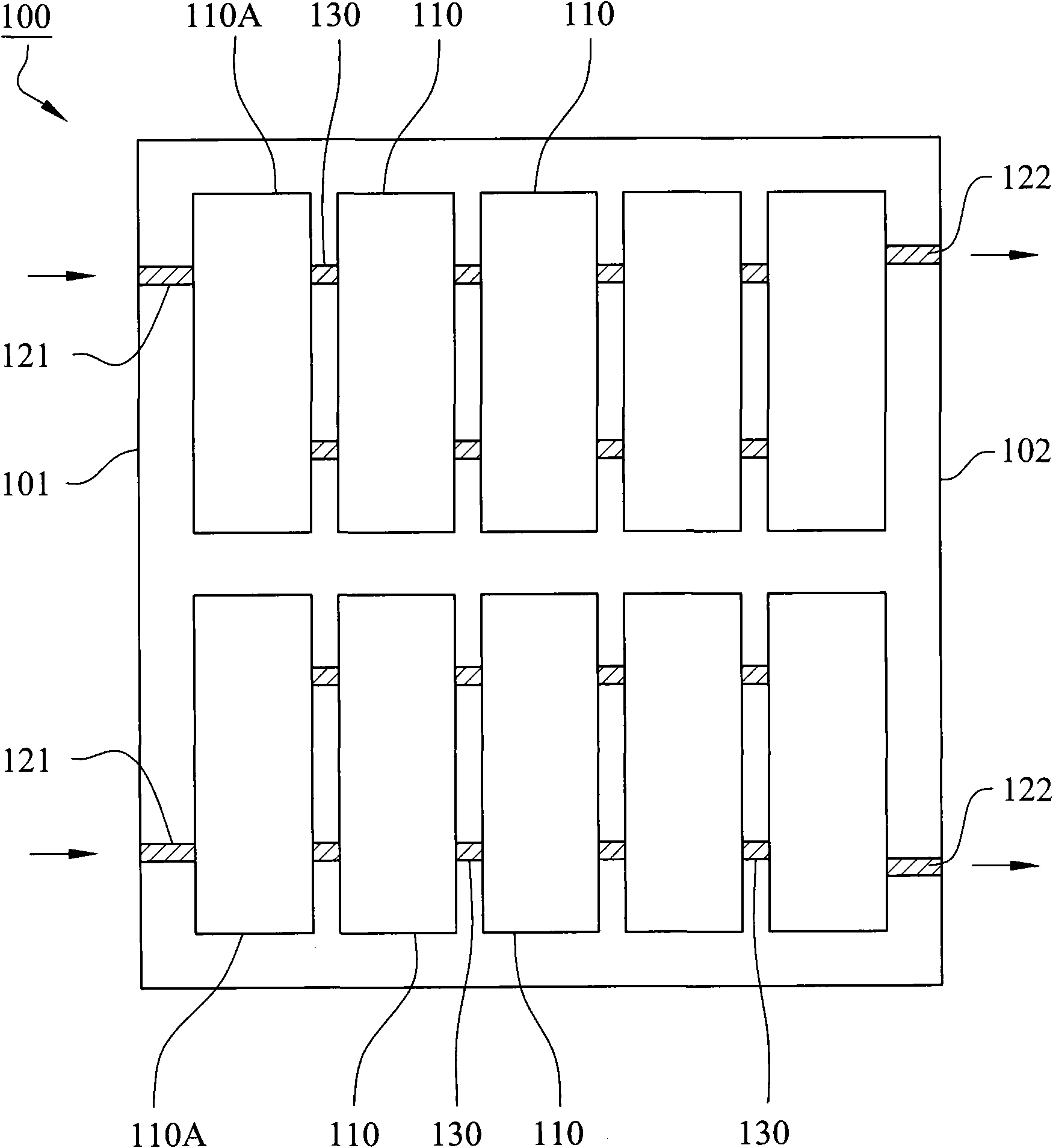
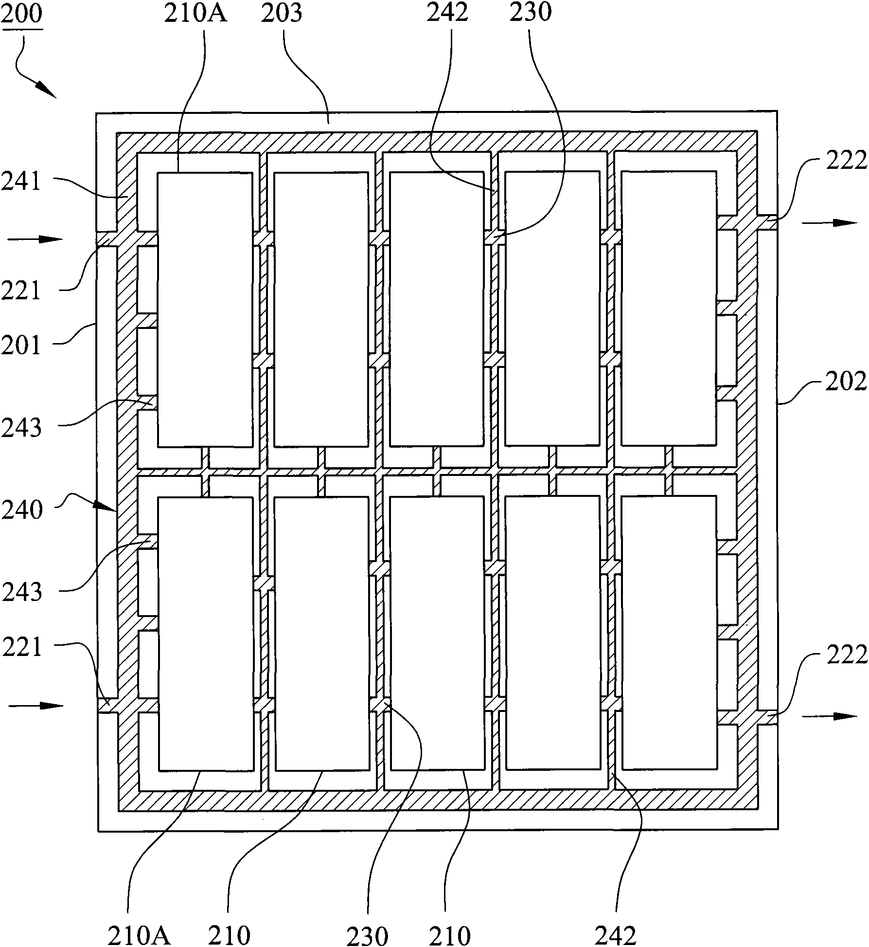
[0040] According to a specific embodiment of the present invention, a substrate panel is illustrated in figure 2 The schematic diagram of the top view and Figure 4A A schematic diagram of a partial cross-section.

[0041] The substrate panel 200 mainly includes two or more substrate strips 210 , two or more electroplating buses 221 and 222 , two or more electroplating serial lines 230 and a current input gate buffer 240 . Usually, the substrate panel 200 can be a large-sized printed circuit board, and the ratio of the long side to the wide side is approximately equal or not more than twice, such as 1:1, 4:3 or 16:10, etc., and is in the form of a panel form.

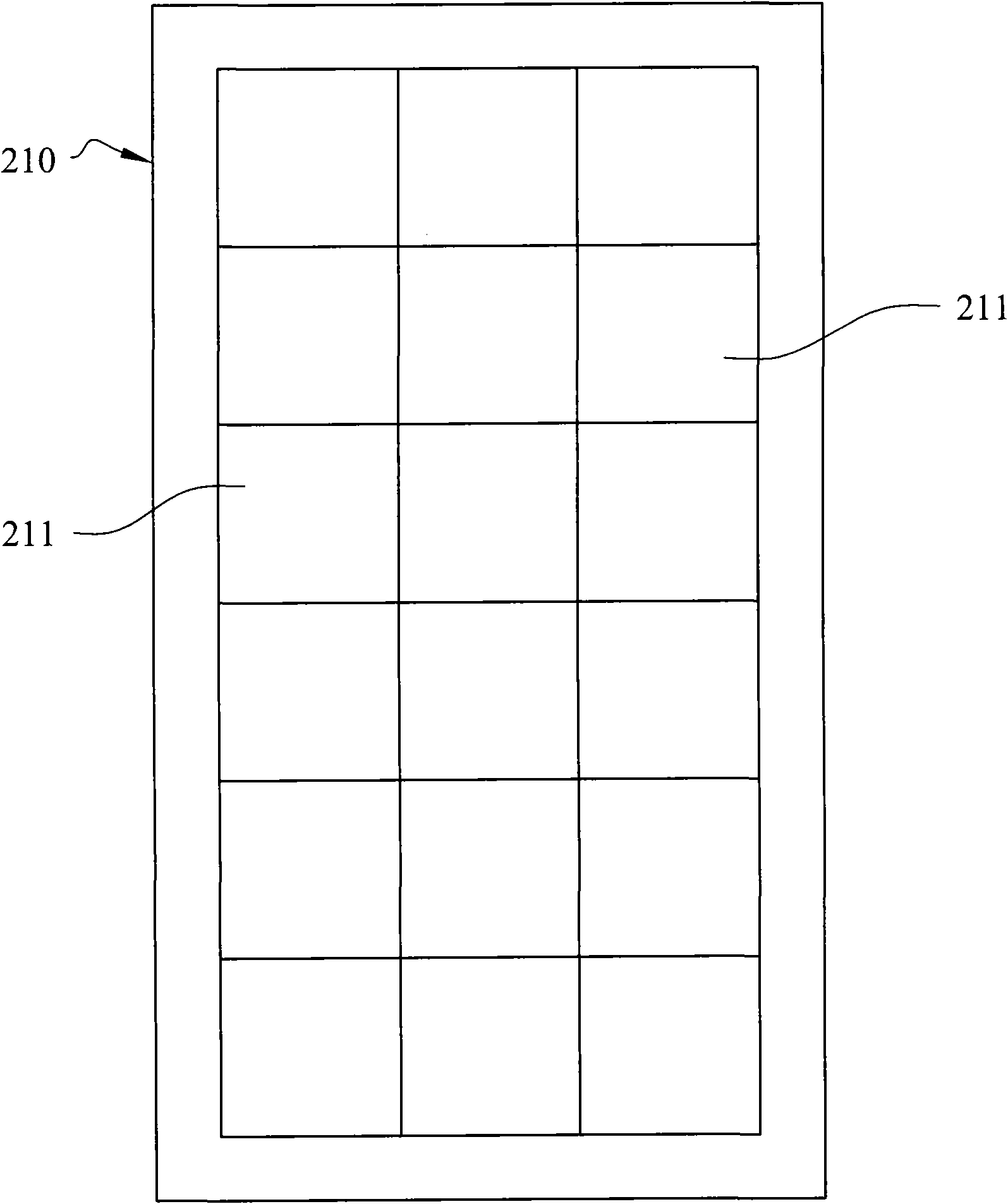
[0042] The substrate strips 210 are arranged in an array on the substrate panel 200 . like image 3 As shown, each substrate bar 210 contains two or more substrate units 211 arranged in an array, and each substrate unit 211 can be used as a chip carrier of a semiconductor package / combined structure, and two or more...


PUM


Abstract

The invention relates to a substrate panel, which mainly comprises two or more than two substrate strips arranged on the substrate panel in an array, two or more than two electroplating buses, two or more than two electroplating string connection wires connected between the substrate strips and connected with two adjacent substrate strips, and a current input gate port buffer area. The electroplating buses connect lateral margins of the substrate panel to the adjacent substrate strips; and the current input gate port buffer area is arranged at a non-substrate strip part of the substrate panel and provided with a current buffer frame and two or more than two net wires, wherein the current buffer frame is in cross connection with the electroplating buses, the net wires are in cross connection with the electroplating string connection wires, and two ends of the net wires are connected to the current buffer frame. Therefore, the current is evenly dispersed to each substrate strip during electroplating, the problem of inconsistent thickness of an electroplating layer due to unevenness of the current density is improved, and instantaneous high current can be buffered and instable voltage can be relaxed to protect internal circuits of the substrate strips.

Description

technical field [0001] The invention relates to a printed circuit board, especially a substrate panel. Background technique [0002] At present, the printed circuit board can be used as a micro-substrate (or referred to as a substrate unit) for carrying chips, and a plurality of micro-substrates arranged in an array are formed in a substrate strip (Substrate Strip). Semiconductor packaging / assembly operations are carried out by substrate strip transfer. In addition, a plurality of substrate strips arranged in an array form a substrate panel (Substrate Panel), so as to facilitate mass production using a printed circuit board process. Usually, before these substrate strips are singulated and separated, the substrate panel will be subjected to an electroplating step in order to plate nickel / gold or other electroplating layers on these substrate strips to prevent oxidation of exposed metal pads and facilitate metal bonding in subsequent processes , such as putting gold wires o...

Claims


Application Information

Patent Timeline
IPC IPC(8): H01L23/498
CPCH01L2924/0002
Inventor 范文正
Owner POWERTECH TECHNOLOGY
Why Eureka
Try Eureka