Liquid crystal display panel

A liquid crystal display panel and liquid crystal layer technology, applied in static indicators, optics, instruments, etc., can solve problems such as low reliability of display panels, interference of electronic products, abnormality of substrate circuits, etc.

Inactive Publication Date: 2010-01-20
WINTEK CORP
View PDF0 Cites 61 Cited by
  • Summary
  • Abstract
  • Description
  • Claims
  • Application Information

AI Technical Summary

Problems solved by technology

However, static electricity in the environment exists all the time, causing almost all electronic products to be disturbed or even damaged by electrostatic discharge
[0003] Traditionally, the two substrates of the liquid crystal display panel often accumulate static charges. When the accumulated static charges are too much, the internal circuits of the substrates will be abnormal or even damaged.
Although traditionally, the liquid crystal display panel has been designed with an electrostatic discharge circuit in the internal circuit of the substrate, its electrostatic protection ability can only prevent static electricity below about 2KV, so that the reliability of the liquid crystal display panel's electrostatic protection ability is not high.

Method used


Image

  • Liquid crystal display panel
  • Liquid crystal display panel
  • Liquid crystal display panel

Examples


no. 1 example

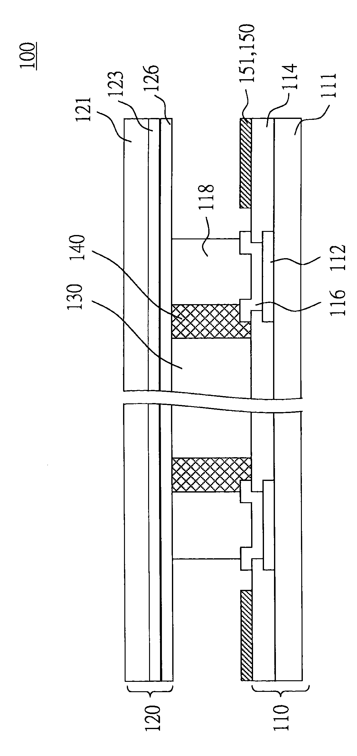
[0045] In the first embodiment, the electrostatic protection structure includes a first wiring. The first wiring is arranged on the thin film transistor substrate and surrounds the edge of the thin film transistor substrate.

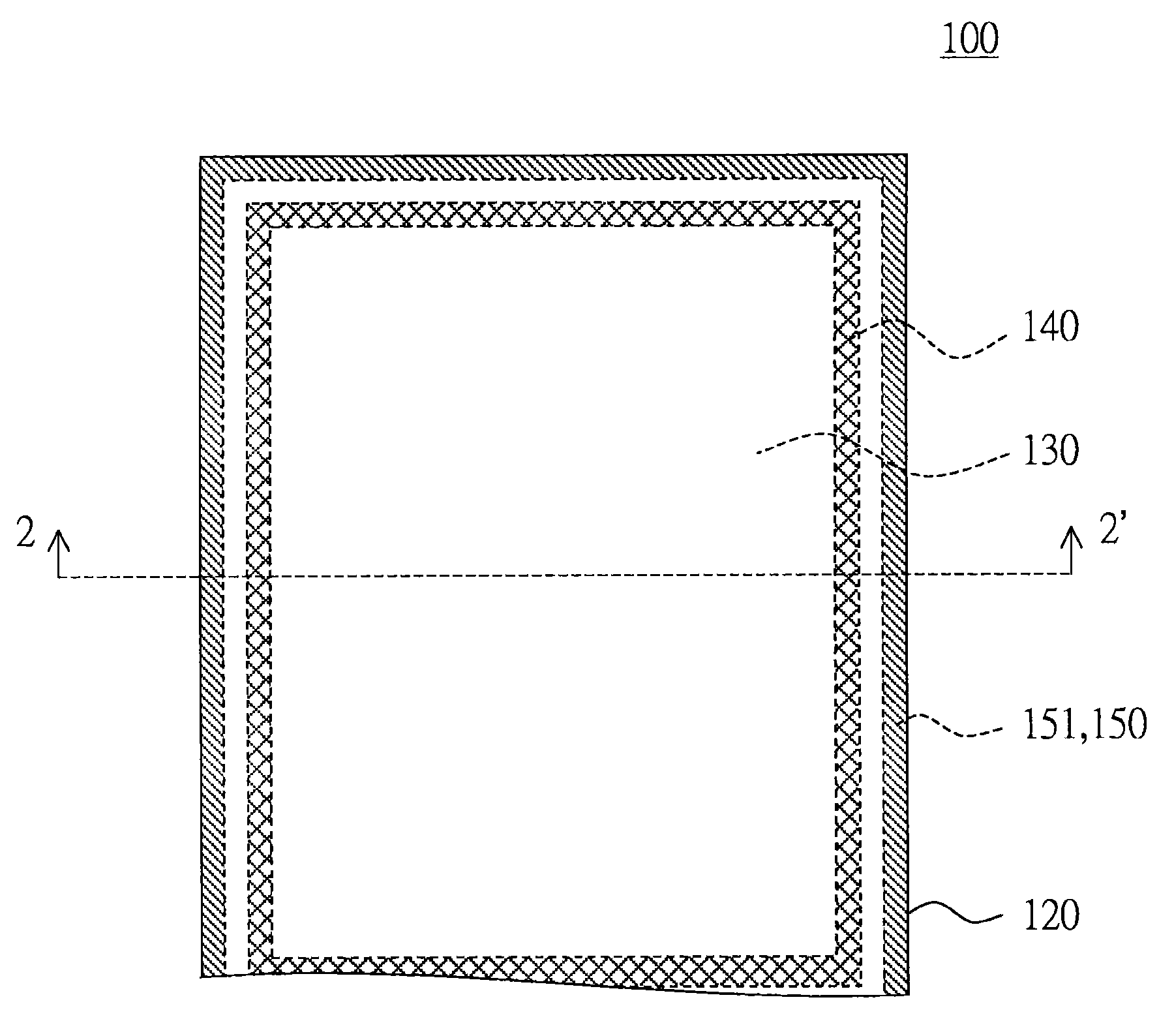
[0046] Please also refer to figure 1 and figure 2 , figure 1 A schematic diagram showing part of a liquid crystal display panel according to the first embodiment of the present invention, figure 2 draw figure 1 The sectional view of the liquid crystal display panel at section line 2-2'. The liquid crystal display panel 100 includes a thin film transistor substrate 110 , a color filter substrate 120 , a liquid crystal layer 130 , a sealant 140 and an electrostatic protection structure 150 . The TFT substrate 110 and the color filter substrate 120 are arranged parallel to each other. The sealant 140 seals the liquid crystal layer 130 between the TFT substrate 110 and the color filter substrate 120 . The area inside the sealant 140 is the display a...

no. 2 example

[0052] The difference between the second embodiment and the above-mentioned first embodiment lies in the arrangement relationship between the common electrode wiring and the electrostatic protection structure. In the second embodiment, the static electricity protection capability of the liquid crystal display panel is further enhanced by changing the arrangement relationship between the common electrode wiring and the static electricity protection structure. Please refer to Figure 5 , which shows a cross-sectional view of a liquid crystal display panel according to a second embodiment of the present invention. Figure 5 can be regarded as figure 2 The similar components use similar symbols, so the function and structural relationship of the similar components will not be repeated below.

[0053] exist Figure 5 Among them, the first trace 251 and the common electrode trace 212 are partially overlapped and electrically insulated, so as to form a capacitive structure at the...

no. 3 example

[0055] The difference between the third embodiment and the above-mentioned second embodiment is that there is a metal layer between the first trace and the common electrode trace. In this embodiment, the equivalent capacitance value of the capacitor structure is increased by using the above metal layer, so as to further enhance the electrostatic protection capability of the liquid crystal display panel. Please refer to Figure 6 , which shows a cross-sectional view of a liquid crystal display panel according to a third embodiment of the present invention. Figure 6 can be regarded as Figure 5 The similar components use similar symbols, so the function and structural relationship of the similar components will not be repeated below.

[0056] exist Figure 6 Among them, the electrostatic protection structure 350 further includes a metal layer 353 located between the first trace 351 and the common electrode trace 312 , and part of the metal layer 353 is covered by the insulat...


PUM


Abstract

The invention discloses a liquid crystal display panel, which comprises a thin film transistor substrate, a color filter substrate, a liquid crystal layer, frame glue and an electrostatic protection structure. The thin film transistor substrate and the color filter substrate are arranged in parallel mutually. The frame glue is used for sealing the liquid crystal layer between the thin film transistor substrate and the color filter substrate. The electrostatic protection structure is positioned in a non-display area outside the frame glue, wherein the electrostatic protection structure comprises a first routing; and the first routing is at least arranged above one of the thin film transistor substrate and the color filter substrate, and encircles the edge of one of the thin film transistor substrate and the color filter substrate.

Description

technical field [0001] The present invention relates to a liquid crystal display panel, and in particular to a liquid crystal display panel with an electrostatic protection structure. Background technique [0002] Today, electronic products have filled every aspect of consumers' lives. However, static electricity in the environment exists all the time, causing almost all electronic products to be disturbed or even damaged by electrostatic discharge. [0003] Traditionally, the two substrates of the liquid crystal display panel often accumulate static charges. When the accumulated static charges are too much, the internal circuits of the substrates will be abnormal or even damaged. Although traditionally, the liquid crystal display panel has been designed with an electrostatic discharge circuit in the internal circuit of the substrate, its electrostatic protection ability can only prevent static electricity below about 2KV, so that the reliability of the liquid crystal displ...

Claims


Application Information

Patent Timeline
Patent Type & Authority Applications(China)
IPC IPC(8): G02F1/133G02F1/1362H01L27/12G02F1/1335
Inventor 黄俊纲吴俊杰苏家莉
Owner WINTEK CORP
Why Eureka
Try Eureka