
Wiring substrate and method of manufacturing the same

A wiring substrate and wiring technology, which is applied in the fields of printed circuit manufacturing, semiconductor/solid-state device manufacturing, printed circuit, etc., can solve problems such as difficult wiring density, and achieve the effect of increasing wiring density

Inactive Publication Date: 2010-01-20
RENESAS ELECTRONICS CORP
View PDF1 Cites 0 Cited by
  • Summary
  • Abstract
  • Description
  • Claims
  • Application Information

AI Technical Summary

Problems solved by technology

As mentioned above, it is difficult to fully guarantee that the wiring density can be increased and the transmission speed of the signal can be adjusted without changing the design of the wiring.

Method used


Image

  • Wiring substrate and method of manufacturing the same
  • Wiring substrate and method of manufacturing the same
  • Wiring substrate and method of manufacturing the same

Examples


Embodiment Construction

[0036] Embodiments of the present invention will be described below with reference to the accompanying drawings. Incidentally, in all drawings, like reference numerals denote like constituent elements, and descriptions of such constituent elements are appropriately omitted.

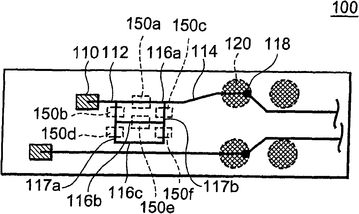
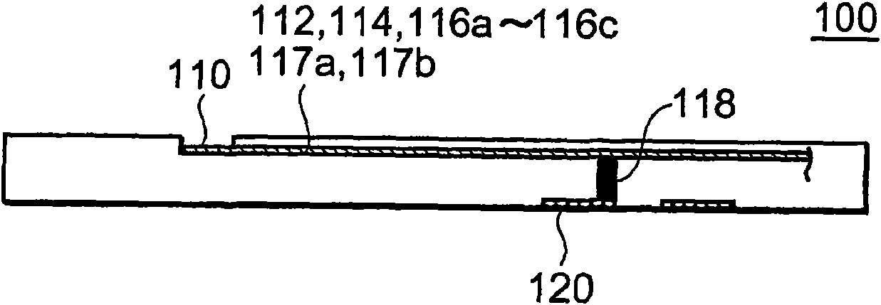
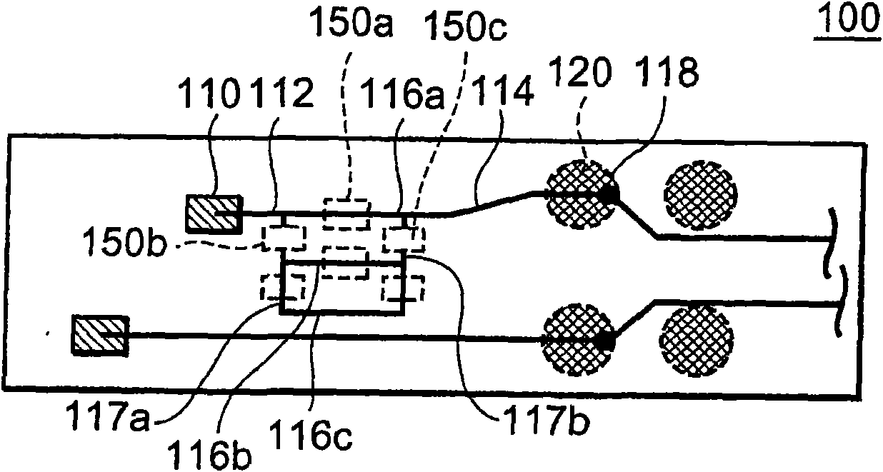
[0037] Figure 1A is an enlarged plan view of an essential part of the wiring substrate 100 in the first embodiment, and Figure 1B yes Figure 1A cross-sectional view. The wiring substrate 100 is provided with a first terminal 110, a second terminal 120, a first wiring 112, a second wiring 114, a plurality of third wirings, and a plurality of fourth wirings. In the example shown in the drawing, a plurality of third wirings and a plurality of fourth wirings are formed by the tenth wiring 117a, the eleventh wiring 117b, and the twelfth wirings 116a to 116c.

[0038] The first terminal 110 is connected to a first electronic component, and the second terminal 120 is connected to a second electronic compone...


PUM


Abstract

Provided is a wiring substrate which enables wiring density to be increased and enables transmission speed of signals to be adjusted without making a design change of wirings. A wiring substrate 100 is provided with a first terminal 110, a second terminal 120, a first wiring 112 and a second wiring 114. The first wiring 112 is such that one end thereof is connected to the first terminal 110, and is formed on the wiring substrate 100. The second wiring 114 is such that one end thereof is connected to the second terminal 120, and is formed on the wiring substrate 100. One end of each of a plurality of third wirings formed on the wiring substrate 100 is connected to the other end of the first wiring 112, and one end of each of a plurality of fourth wirings formed on the wiring substrate 100 is connected to the other end of the second wiring 114. The other end of at least one third wiring and the other end of at least fourth wiring are connected together.

Description

technical field [0001] The present invention relates to a wiring substrate capable of increasing the wiring density and adjusting the transmission speed of signals without changing the design of the wiring and a method of manufacturing the wiring substrate. Background technique [0002] In a semiconductor chip, in some cases, it is necessary to make the transmission speeds of a plurality of signals equal to each other. In this case, in designing a semiconductor chip, a wiring substrate, a motherboard, etc., the wiring lengths are made equal, thereby preventing a difference in transmission speed of signals. However, even when such a design is performed, a difference in the transmission speed of a signal sometimes occurs when a product is actually manufactured. [0003] The following technology is disclosed in Japanese Patent Laid-Open No. 2005-322814. That is, for wiring where a signal propagates faster than the standard transmission speed, capacitance is increased by conne...

Claims


Application Information

Patent Timeline
Patent Type & Authority Applications(China)
IPC IPC(8): H01L23/48H01L23/12H01L21/48H01L21/66
CPCH01L2224/484H01L2924/12041H01L2924/01015H01L2224/48091H05K1/0237H01L2924/01004H01L2924/01078H01L2924/01006H05K2203/175H01L2224/48228H01L24/48H01L24/16H01L2924/01079H01L2924/15183H01L2924/15311H01L2224/16237H01L2924/01005H01L2224/13099H01L2224/45144H05K1/029H01L2924/30107H05K2201/10674H01L2924/014H01L2224/49175H01L24/49H01L2924/30105H01L2224/48599H01L2224/48227H01L2924/01033H01L23/49838H01L2924/00014H01L24/45H01L2224/05554H01L2224/04042H01L2924/00011H01L2924/00H01L2224/05599H01L2224/0401Y10T29/49147Y10T29/49004
Inventor 石塚伸彦
Owner RENESAS ELECTRONICS CORP
Learn More