Semiconductor substrate for solar cell and method for manufacturing same

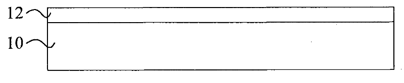
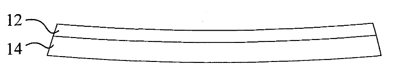
A solar cell, semiconductor technology, applied in the direction of semiconductor devices, final product manufacturing, sustainable manufacturing/processing, etc., can solve problems such as disadvantage, warpage of thin silicon wafers 14, etc.

Inactive Publication Date: 2011-09-07
KUNSHAN ZHONGCHEN SILICON CO LTD
View PDF0 Cites 0 Cited by
  • Summary
  • Abstract
  • Description
  • Claims
  • Application Information

AI Technical Summary

Problems solved by technology

However, the thin silicon wafer 14 will be warped due to excessive temperature during the thermal oxidation process, which is not conducive to the subsequent process.

Method used


Image

  • Semiconductor substrate for solar cell and method for manufacturing same
  • Semiconductor substrate for solar cell and method for manufacturing same
  • Semiconductor substrate for solar cell and method for manufacturing same

Examples


Embodiment Construction

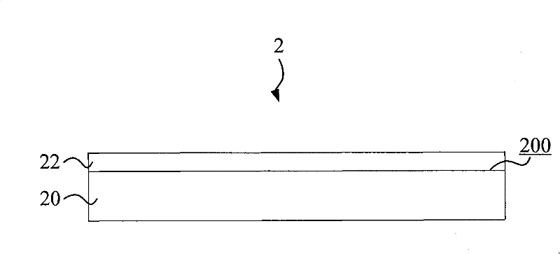
[0018] see figure 2 , figure 2 A semiconductor substrate 2 according to an embodiment of the invention is shown. The semiconductor substrate 2 can be used for solar cells.

[0019] Such as figure 2 As shown, the semiconductor substrate 2 includes a substrate 20 and a surface passivation layer 22 . The substrate 20 has an upper surface 200 .

[0020] In a specific embodiment, the substrate 20 may be made of silicon and the thickness of the substrate 20 is substantially equal to or less than 300 μm. In other words, the substrate 20 can be a thin substrate 20 .

[0021] The surface passivation layer 22 can be formed on the upper surface 200 of the substrate 20 by an atomic layer deposition process, a plasma-enhanced atomic layer deposition process or a plasma-assisted atomic layer deposition process. A layer deposition process and a plasma-enhanced atomic layer deposition process or a combined process of an atomic layer deposition process and a plasma-assisted atomic lay...


PUM


Abstract

The present invention discloses a semiconductor substrate for a solar cell and a method for manufacturing the same. The semiconductor substrate of the present invention comprises a substrate and a surface passivation layer. The substrate has an upper surface. The surface passivation layer is formed on the upper surface of the substrate by an atom layer depositing process and / or a plasma-aided atom depositing process.

Description

technical field [0001] The invention relates to a semiconductor substrate, in particular to a semiconductor substrate for solar cells. Background technique [0002] Solar cells have been widely used because they convert energy from a light source (eg, sunlight) into electricity to power electronic devices such as computers, computers, heaters, and the like. [0003] So far, although silicon solar cells are the mainstream in the market, the problem of shortage of silicon source materials is becoming more and more serious. Therefore, in order to save materials and costs, the development of thin solar cells (for example, solar cells using thin silicon wafers as substrates) has become a trend. At the same time, in response to the development of thin solar cells, thin silicon wafers have been manufactured and applied to solar cells. [0004] The principle of solar cells is that photons enter the silicon substrate and are absorbed by the silicon substrate to transfer the energy ...

Claims


Application Information

Patent Timeline
Patent Type & Authority Patents(China)
IPC IPC(8): H01L31/02H01L31/18
CPCY02P70/50
Inventor 陈敏璋徐文庆何思桦
Owner KUNSHAN ZHONGCHEN SILICON CO LTD
Why Eureka
Try Eureka