

Packaging structure of wafer layered electromagnetic shielding circuit
A technology of electromagnetic shielding and packaging structure, which is applied in the direction of circuits, electrical components, metal processing, etc., can solve the problems of insufficient cutting of packaging film, prolong the packaging process of electromagnetic shielding lines, etc., and achieve the effect of sufficient cutting
- Summary
- Abstract
- Description
- Claims
- Application Information
AI Technical Summary
Problems solved by technology
Method used
Image

Examples
Embodiment Construction
[0037] The following will clearly and completely describe the technical solutions in the embodiments of the present invention with reference to the accompanying drawings in the embodiments of the present invention. Obviously, the described embodiments are only some, not all, embodiments of the present invention. Based on the embodiments of the present invention, all other embodiments obtained by persons of ordinary skill in the art without making creative efforts belong to the protection scope of the present invention.
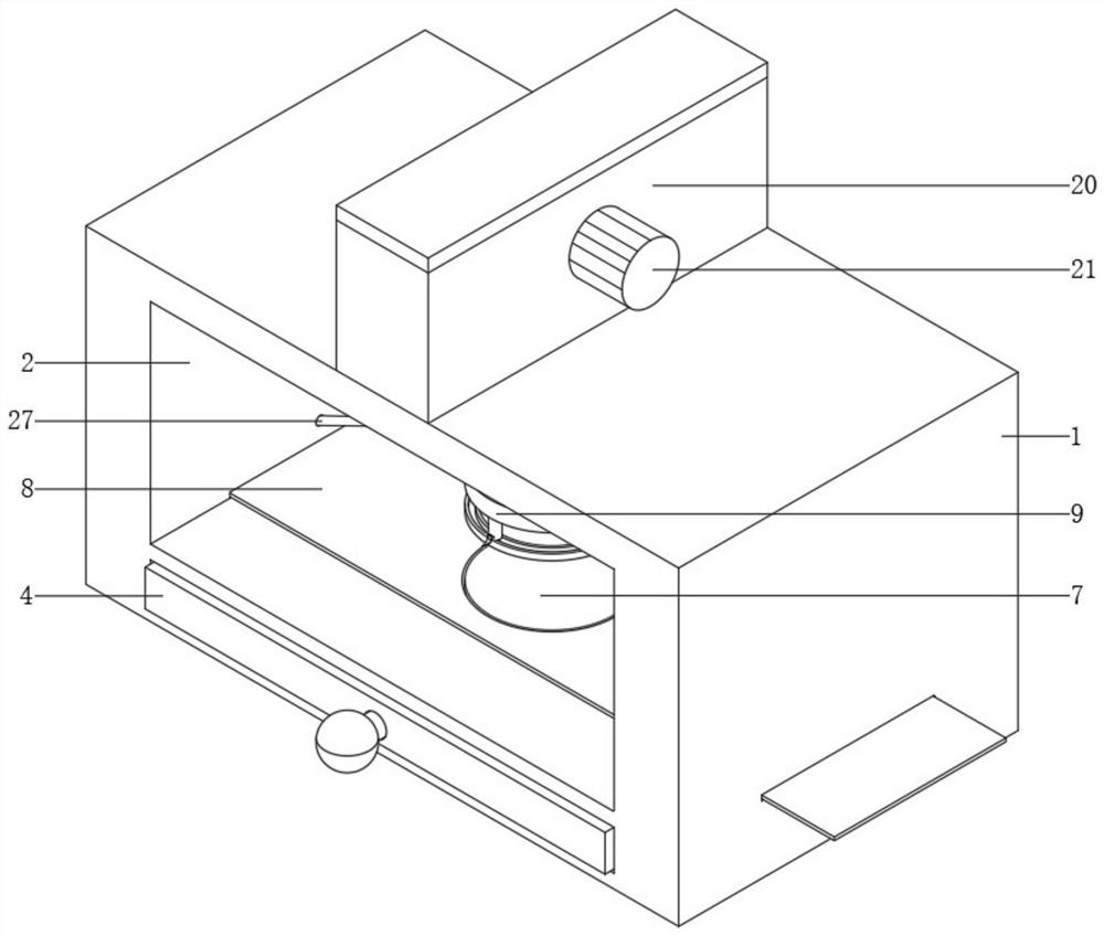
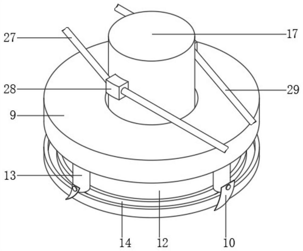
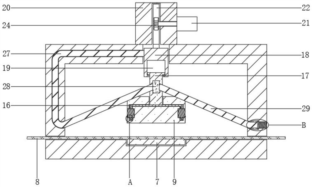
[0038] see Figure 1-10As shown, the packaging structure of the wafer layered electromagnetic shielding circuit includes a fixed frame 1, the fixed frame 1 is an existing alloy frame, the front of the fixed frame 1 is provided with an operation chamber 2, and the opening of the operation chamber 2 can be It is convenient for the staff to observe the packaging situation of the wafer body 7 in real time. The bottom end of the operation chamber 2 is provided with...
PUM
 Abstract
Description
Claims
Application Information