Semiconductor memory device

A storage device and semiconductor technology, applied in information storage, static memory, digital memory information and other directions, can solve the problems of time delay in writing, inability to read data, wrong writing, etc., to ensure the read and write operation margin. Effect

Inactive Publication Date: 2013-01-02
RENESAS ELECTRONICS CORP
View PDF2 Cites 0 Cited by
  • Summary
  • Abstract
  • Description
  • Claims
  • Application Information

AI Technical Summary

Problems solved by technology

However, the data held by the memory cell 105s that selects the column and selects the word line and the memory cell 105n that selects the column and does not select the word line are different, and the access transistors Tr1n, Tr2n of the non-selected cell 105n and the bit line pair (D, DB) under the situation that is not completely isolated, will be changed to the bit line of low level ( Figure 9 The middle is the data line DB) is kept as high level by non-selection unit 105n, and will be kept as high level bit line ( Figure 9 In the middle, the data line D) is lowered to a low level by the non-selection unit 105n, so a sufficient potential difference is not generated on the bit line pair (D, DB), and there is a case where the sense amplifier 108 cannot read correct data.
[0024] In the writing operation, according to the data written in the write buffer 109, one of the precharged bit line pairs (D, DB) is lowered to a low level, and the other is kept at a precharged high level potential, but the column is selected. And the memory cells 105n of the non-selected word line all keep the data opposite to the write data, and when the access transistors Tr1n, Tr2n and the bit line pair (D, DB) are not completely isolated, the write cache 109 will drop to low power. The flat bit line is raised to a high level, so that the bit line to be kept high by the cache memory 109 is lowered to a low level, so there will be a delay in writing completion time and wrong writing.

Method used


Image

  • Semiconductor memory device
  • Semiconductor memory device
  • Semiconductor memory device

Examples


Embodiment 1

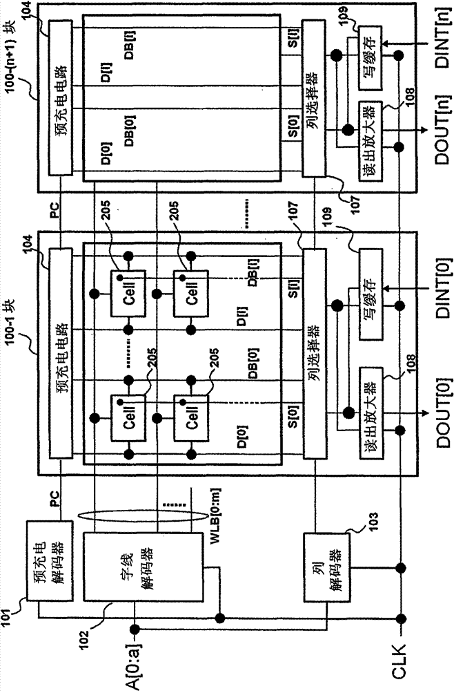
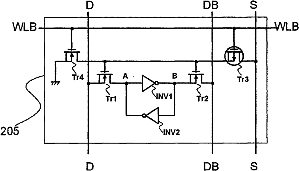
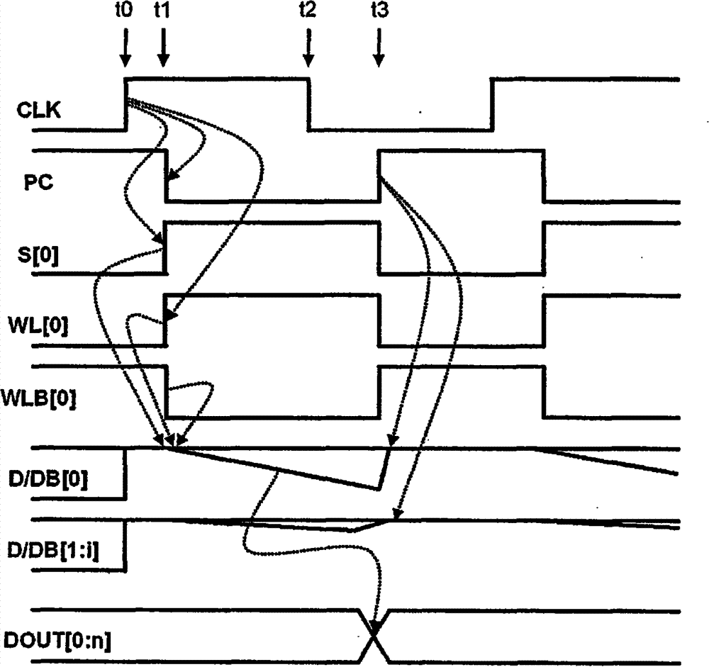
[0053] figure 1 It is an overall block diagram of the semiconductor memory device of the first embodiment. figure 1 The semiconductor memory device is composed of n+1 (bit) memory blocks of 100-1 to 100-(n+1). Each memory block is composed of i+1 columns from 0 to i, and the address is specified and accessed through m+1 word lines from 0 to m, so the whole is [(m+1)×(i+1)] word The configuration of ×(n+1) bits (digits). In addition, corresponding to this configuration, a precharge decoder 101 , a word line decoder 102 , and a column decoder 103 are provided. In addition, each memory block is provided with: memory cells 205 arranged as (m+1)×(i+1), AND charging circuits 104, column selectors 107, sense amplifiers 108, and write buffers respectively arranged according to each bit line. 109. Further, the memory cells 205 are connected to column selection lines S[0:i]. By this column selection line S[0:i], the bit line pairs other than the selected bit line pair are separat...

Embodiment 2

[0070] Figure 4 It is an overall circuit block diagram showing a semiconductor memory device according to Embodiment 2 of the present invention. In the second embodiment, the parts having basically the same structure as that of the first embodiment are given the same symbols in the drawings as those of the first embodiment, and detailed description thereof will be omitted. Figure 4 and figure 1 The difference is that the memory blocks (100-1 to 100-(n+1)) are not only wired with the word line (logic inversion) WLB[0:m], but also wired with the word line (positive logic) WL[ 0:m]. Other constitution and embodiment 1 figure 1 basically the same.

[0071] Figure 5 yes means Figure 4 A block diagram of the construction of the storage unit 305 is shown. and Example 1's figure 2Compared with the memory cell of the above, the difference is that, between the column selection line S[0:i] and the gates of the access transistors Tr1 and Tr2, a second access transistor cont...


PUM


Abstract

A semiconductor memory device includes a plurality of memory cells 205 provided corresponding to nodes of a plurality of word lines (WLBk, WLBk+1) and a plurality of bit line pairs (D1, DB1, D1+1, DB1+1). And column selection lines (S1, S1+1) are provided corresponding to each of the bit line pairs. Each of the memory cell includes an inverter (INV3) receiving power from the column selection line, and having its input connected to the word line and its output connected to gates of access transistors. Only the access transistors of a memory cell whose word line and column selection line are simultaneously selected are turned on.

Description

technical field [0001] The present invention relates to a semiconductor memory device. In particular, it relates to a semiconductor memory device using an SRAM cell. Background technique [0002] In recent semiconductor integrated circuits, the scale of a system mounted on a single-chip semiconductor integrated circuit has increased along with an increase in the degree of integration due to miniaturization, and its operating speed has also tended to increase. Furthermore, in the field of application of semiconductor integrated circuits, the market for mobile devices such as mobile phones, digital cameras, and PDAs is growing rapidly. In such application fields as mobile devices, power saving becomes a great added value of products. In semiconductor integrated circuits for memory, mounting capacity is also increasing year by year, and power saving technology has become a major issue. Especially in SRAM, reduction of charge and discharge current of a bit line (Digit line), ...

Claims


Application Information

Patent Timeline
Patent Type & Authority Patents(China)
IPC IPC(8): G11C11/412G11C11/417
CPCG11C8/08G11C11/412
Inventor 宇野和正
Owner RENESAS ELECTRONICS CORP
Why Eureka
Try Eureka