Panel antenna and wireless communication device

A technology for wireless communication devices and flat-panel antennas, which is applied in the directions of antennas, resonant antennas, radiating element structures, etc., can solve the problems of more manpower, antenna size, material costs, and labor assembly costs, and achieves restraint of materials and manpower. Cost, reduce material cost and labor assembly cost, suppress the effect of substantial increase

Active Publication Date: 2010-02-24
ASUSTEK COMPUTER INC
View PDF0 Cites 8 Cited by
  • Summary
  • Abstract
  • Description
  • Claims
  • Application Information

AI Technical Summary

Problems solved by technology

[0004] However, based on the current cost of a single antenna of about 20-30 Taiwan dollars, the cost of the antenna part of the wireless communication device must cost 100-150 Taiwan dollars
In addition, with the increase of built-in antennas, system manufacturers must spend more manpower and time to assemble these antennas
In other words, when multiple antennas are built into a wireless communication device, its antenna size, material cost and labor assembly cost will increase significantly

Method used


Image

  • Panel antenna and wireless communication device
  • Panel antenna and wireless communication device
  • Panel antenna and wireless communication device

Examples


Embodiment Construction

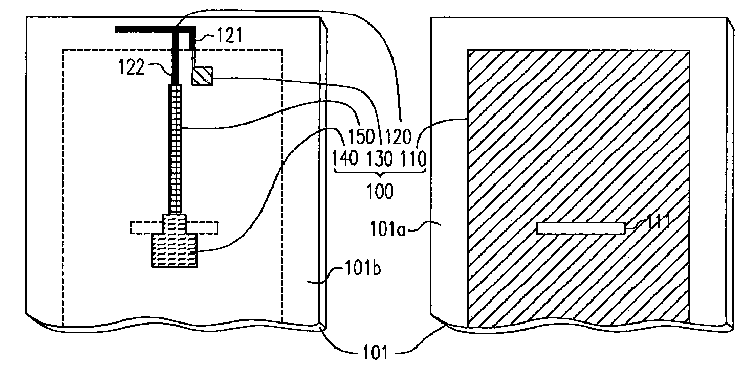
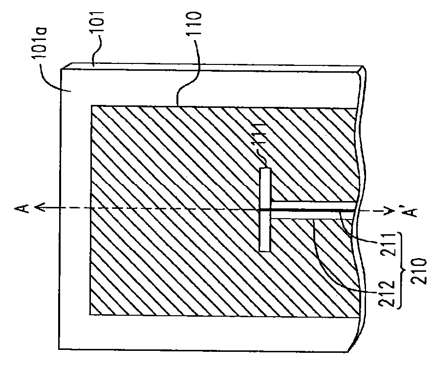
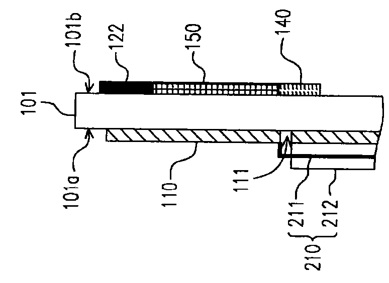
[0032] figure 1 Shown is a schematic structural view of a panel antenna according to an embodiment of the present invention, wherein the panel antenna 100 is disposed on a board 101, and the board 101 has a first surface 101a and a second surface 101b.

[0033] It should be noted that, in this embodiment, the board 101 may be a printed circuit board, and the first surface 101a and the second surface 101b are parallel to each other. However, those skilled in the art can also apply the panel antenna 100 on any panel with two surfaces according to design requirements. In other words, although this embodiment has described a possible form of the board 101 , it is not intended to limit the present invention.

[0034] Please continue to refer to figure 1 , the panel antenna 100 includes a metal layer 110 , an antenna body 120 , a step impedance element 130 , a coupling element 140 and a matching element 150 . Wherein, the metal layer 110 is disposed on the first surface 101a, and...


PUM


Abstract

The invention relates to a panel antenna and a wireless communication device, in particular to a panel antenna without a through hole structure. The panel antenna is arranged on a plate. The plate is provided with a first surface and a second surface. The panel antenna comprises a metal layer, an antenna body, a stepped impedance element, a coupling element and a matching element. The metal layeris arranged on the first surface and is provided with a groove body for exposing the first surface. The antenna body, the stepped impedance element, the coupling element and the matching element are arranged on the second surface. Apart from a feed-in end of the antenna body, the antenna body corresponds to the periphery of the metal layer. The stepped impedance element and the matching element correspond to the metal layer, while the coupling element corresponds to the groove body. The matching element is electrically connected between the coupling element and the feed-in end of the antenna body to be used as impedance match. The stepped impedance element is electrically connected with a grounding terminal of the antenna body and has a transmission zero point in a radio-frequency range operated by the antenna body.

Description

technical field [0001] The present invention relates to a flat-panel antenna and a wireless communication device, and in particular to a flat-panel antenna and a wireless communication device that do not need a through-hole structure. Background technique [0002] With the progress and development of wireless transmission hardware equipment and technology, Multi Input Multi Output (MIMO) technology has become an important indicator of high-performance wireless technology, and will gradually become the mainstream of future wireless communication. Different from the traditional single-antenna operation design in the past, MIMO technology uses multiple antennas to operate simultaneously to achieve multi-path transmission wireless networks. In addition, MIMO technology has the advantages of improving the transmission speed and receiving range of wireless networks. [0003] In a wireless network based on MIMO technology, a wireless communication device must be equipped with mult...

Claims


Application Information

Patent Timeline
Patent Type & Authority Applications(China)
IPC IPC(8): H01Q1/38H01Q9/04H01Q13/08
Inventor 赖明佑陈泓翔邱杨博王俊雄
Owner ASUSTEK COMPUTER INC
Why Eureka
Try Eureka