Array substrate for liquid crystal display device and manufacturing method of the same

An array substrate and substrate technology, which is applied in the field of liquid crystal display devices, can solve the problems of not being able to refresh the carrier wave smoothly and reducing the image quality, etc.

Active Publication Date: 2010-03-10
LG DISPLAY CO LTD
View PDF2 Cites 20 Cited by
  • Summary
  • Abstract
  • Description
  • Claims
  • Application Information

AI Technical Summary

Problems solved by technology

[0032] Therefore, the carrier waves induced in the color filter patterns 96a, 96b, and 96c cannot be refreshed smoothly.
This results in afterimages or banding spots according to the color filter patterns 96a, 96b, and 96c, thereby degrading the image quality

Method used


Image

  • Array substrate for liquid crystal display device and manufacturing method of the same
  • Array substrate for liquid crystal display device and manufacturing method of the same
  • Array substrate for liquid crystal display device and manufacturing method of the same

Examples


Embodiment Construction

[0052] Reference will now be made in detail to embodiments of the invention, examples of which are illustrated in the accompanying drawings.

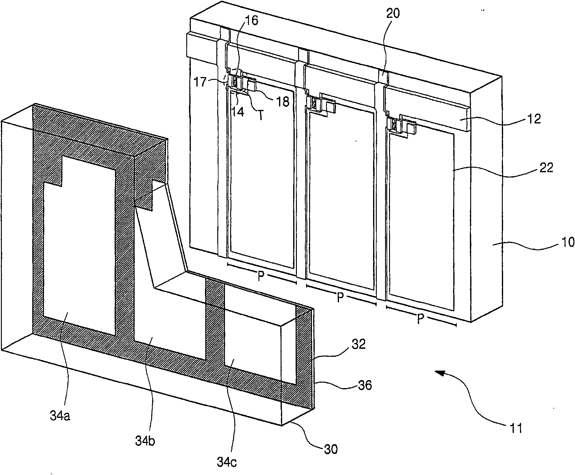
[0053] Figure 5 is an equivalent circuit of the LCD device according to the first embodiment of the present invention.

[0054] exist Figure 5 Among them, the gate lines G1, G2, G3 to Gn (n is a natural number) are formed along the first direction and are spaced apart from each other. The data lines D1, D2, D3 to Dm (m is a natural number) are formed along the second direction and cross the gate lines G1, G2, G3 to Gn to define the pixel region P.

[0055] A thin film transistor T and a liquid crystal capacitor C are formed at each pixel area P. LC and the storage capacitor C ST . The thin film transistor T is connected to a corresponding gate line G1, G2, G3 or Gn and a corresponding data line D1, D2, D3 or Dm. storage capacitor C ST connected in essentially parallel to the liquid crystal capacitor C LC .

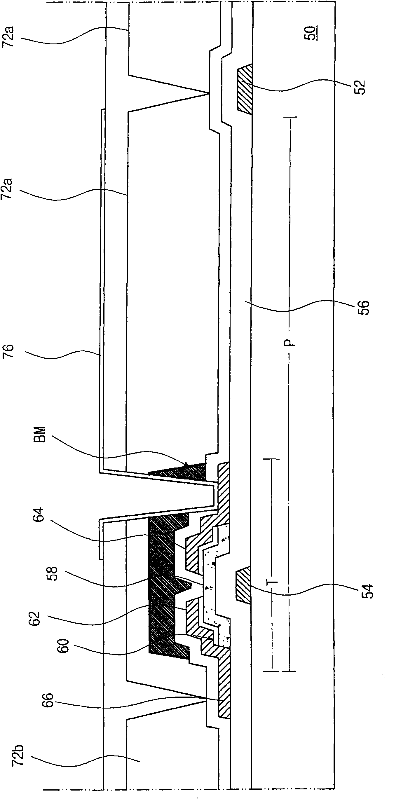
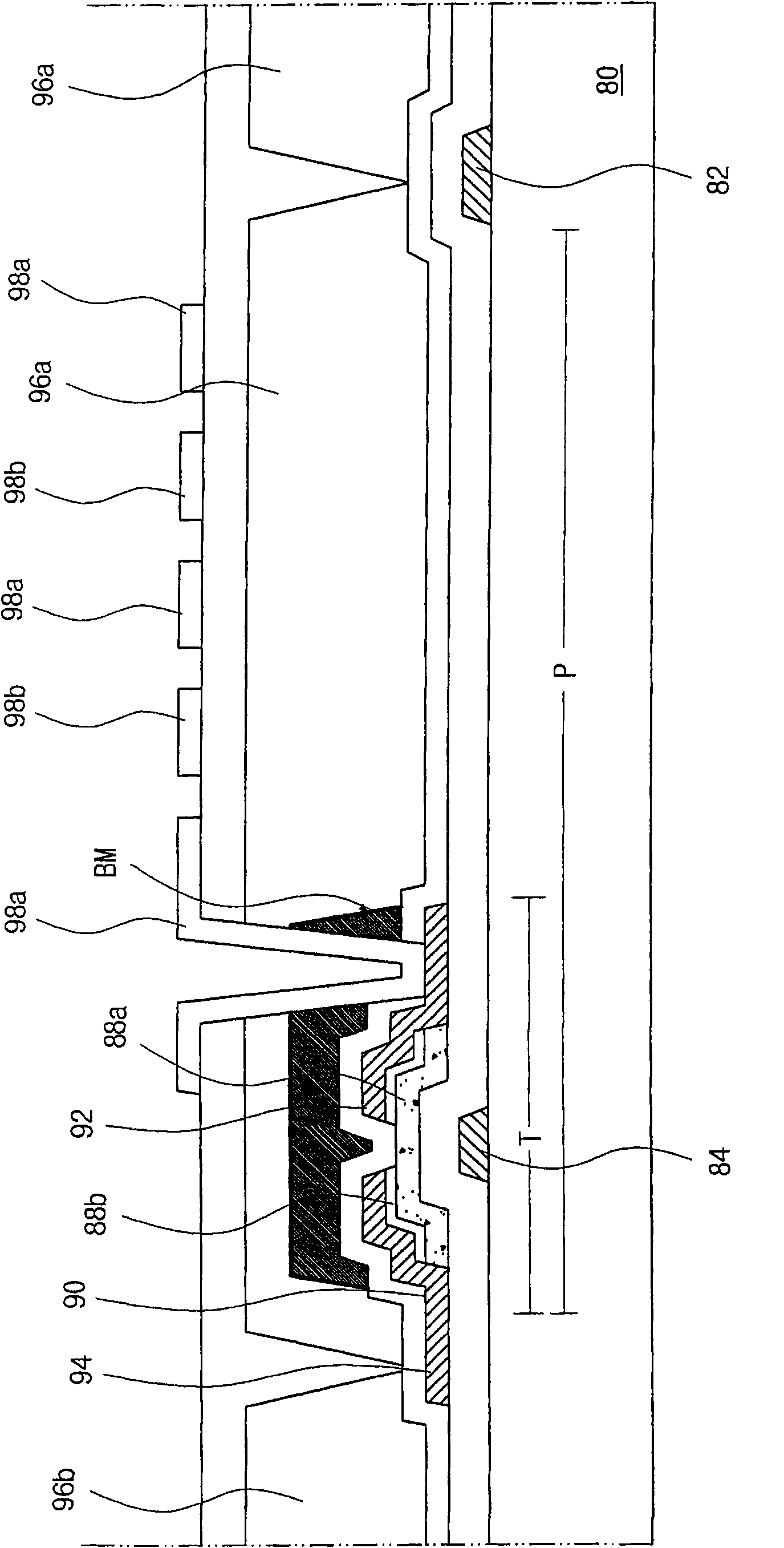
[0056] The color fi...


PUM


Abstract

An array substrate for a COA(Color filter On Array)-IPS(In-Plane Switching) mode LCD is provided to offer a refresh structure according to colors in consideration of different dielectric constants ofred, green, and blue color filters, thereby improving the uniformity of display quality. A plurality of gate lines(G1-Gn) and a plurality of data lines(D1-Dn) cross each other to define pixel regions.A liquid crystal capacitor(CLC) and a storage capacitor(Cst) connected to the liquid crystal capacitor in parallel are formed within each of the pixel regions. Color filters are formed for the pixelregions respectively such that one color filter having a specific color corresponds to one pixel region. First, second, and third common lines(108a,108b,108c) are formed within pixel regions corresponding to red, green, and blue color filters(130a,130b,130c), respectively. The first, second, and third common lines are connected to a separate common electric power. Different common voltages are applied to the pixel regions connected to the first, second, and third common lines to compensate for differences of pixel voltages due to different dielectric constants of the color filters.

Description

[0001] This application is a divisional application of an invention patent application with the application number 200710307381.8, the filing date is December 29, 2007, and the invention title is "Array Substrate for Liquid Crystal Display Device and Method for Manufacturing the Array Substrate". technical field [0002] The present invention relates to a liquid crystal display (LCD) device, and more specifically, to an array substrate for a liquid crystal display device and a manufacturing method thereof. Background technique [0003] Liquid crystal display (LCD) devices are driven based on optical anisotropy and polarization characteristics of liquid crystal materials. The shape of the liquid crystal molecules is long and thin, and the liquid crystal molecules are regularly arranged along the alignment direction. Light passes through the LCD device along the long and thin shape of the liquid crystal molecules. The alignment of liquid crystal molecules depends on the stren...

Claims


Application Information

Patent Timeline
Patent Type & Authority Applications(China)
IPC IPC(8): G02F1/1333G02F1/1362G02F1/1368G02F1/1343G09G3/36
CPCG02F1/134363G02F1/13458G02F1/136213G02F1/136286G02F1/1368
Inventor 蔡基成
Owner LG DISPLAY CO LTD
Why Eureka
Try Eureka