Unlock instant, AI-driven research and patent intelligence for your innovation.

High-precision voltage reference circuit

A voltage reference, high-precision technology, applied in the direction of adjusting electrical variables, control/regulation systems, instruments, etc., can solve the problem of low precision, achieve high output impedance, meet power consumption requirements, and stabilize the drain current

Inactive Publication Date: 2010-03-10
西安龙腾微电子科技发展有限公司
View PDF1 Cites 8 Cited by
  • Summary
  • Abstract
  • Description
  • Claims
  • Application Information

AI Technical Summary

Problems solved by technology

[0013] In order to overcome the deficiency of the low accuracy of the voltage reference circuit in the prior art, the present invention provides a high-precision voltage reference circuit, in which the depletion NMOS transistor M4 can provide a stable current source, and the gate of the enhancement NMOS transistor M5 generates Stable Voltage Reference

Method used


Image

  • High-precision voltage reference circuit
  • High-precision voltage reference circuit
  • High-precision voltage reference circuit

Examples


Embodiment 1

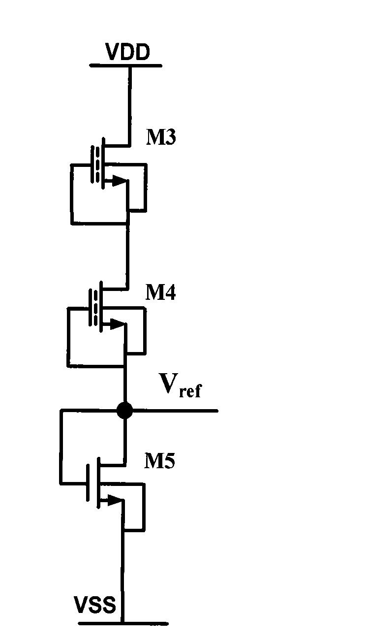
[0022] Embodiment 1: refer to figure 1 , The voltage reference circuit is composed of a depletion NMOS transistor M3 and a depletion NMOS transistor M4, and an enhancement NMOS transistor M5. The drain of the depletion NMOS transistor M3 is connected to the positive power supply VDD, the gate of the depletion NMOS transistor M3 is connected to the source and is connected to the drain of the depletion NMOS transistor M4. The gate and source of the depletion NMOS transistor M4 are connected and connected to the drain of the enhancement NMOS transistor M5. The gate of the enhanced NMOS transistor M5 is connected to the drain, and the source of the enhanced NMOS transistor M5 is connected to the negative power supply VSS. The gate of the enhancement NMOS transistor M5 is the output terminal of the voltage reference. The substrates of all NMOS transistors are connected to their respective sources.

[0023] The sources of the depletion NMOS transistor M3 , the depletion NMOS tra...

Embodiment 2

[0035] Embodiment 2: refer to figure 2 , A voltage reference circuit that outputs a low voltage reference. The circuit is composed of a depletion NMOS transistor M3 and a depletion NMOS transistor M4, and an enhancement NMOS transistor M5. The drain of the depletion NMOS transistor M3 is connected to the positive power supply VDD, and the gate and source of the depletion NMOS transistor M3 are connected to the drain of the depletion NMOS transistor M4. The gate of the depletion NMOS transistor M4 is connected to the source of the enhancement NMOS transistor M5, and the source of the depletion NMOS transistor M4 is connected to the drain of the enhancement NMOS transistor M5. The gate of the enhanced NMOS transistor M5 is connected to the drain, and the source of the enhanced NMOS transistor M5 is connected to the negative power supply VSS. The gate of the enhancement NMOS transistor M5 is the output terminal of the voltage reference. The substrates of all CMOS transistors ...


PUM


Abstract

The invention discloses a high-precision voltage reference circuit comprising a depletion type NMOS transistor M4 and an enhanced NMOS transistor M5. The high-precision voltage reference circuit is characterized by also comprising a depletion type NMOS transistor M3; a drain electrode of the depletion type NMOS transistor M3 is connected with a positive power supply VDD; a grid electrode and a source electrode of the depletion type NMOS transistor M3 are connected with a drain electrode of the depletion type NMOS transistor M4; a grid electrode and a source electrode of the depletion type NMOStransistor M4 are connected with a drain electrode of the enhanced NMOS transistor M5; a grid electrode and a drain electrode of the enhanced NMOS transistor M5 are connected; a source electrode of the enhanced NMOS transistor M5 is connected with a negative power supply VSS; and the grid electrode of the enhanced NMOS transistor M5 is an output end of voltage reference. The depletion type NMOS transistor M3 and the depletion type NMOS transistor M4 form a common source and grid circuit which has high output impedance, thereby stabilizing the output of the voltage reference.

Description

technical field [0001] The invention relates to a voltage reference circuit, in particular to a high-precision voltage reference circuit. Background technique [0002] refer to Figure 4 , the document "Chinese Patent No. ZL96103673.7" discloses a voltage reference circuit, which is composed of a depletion NMOS transistor M4, an enhancement NMOS transistor M5, positive power supply VDD and negative power supply VSS. The drain of the depletion NMOS transistor M4 is connected to the positive power supply VDD, and the gate, source and substrate are connected together and connected to the drain of the enhancement NMOS transistor M5. The gate and the drain of the enhancement NMOS transistor M5 are connected together, the source and the substrate are connected and then connected to the negative power supply VSS. The connection point between the source of the depletion NMOS transistor M4 and the drain of the enhancement NMOS transistor M5 is the output terminal of the voltage refe...

Claims


Application Information

Patent Timeline
IPC IPC(8): G05F3/24
Inventor 刘成魏廷存孙井龙
Owner 西安龙腾微电子科技发展有限公司