Method and system for switching main and backup clocks

A master/standby switchover and clock switchover technology, applied in transmission systems, digital transmission systems, electrical components, etc., can solve problems such as discontinuity of clock phases, complex connections between master and standby boards, hidden dangers in reliability, etc., and achieve simple structure, Phase and system stability and good reliability

Active Publication Date: 2010-03-10
ZTE CORP
View PDF0 Cites 26 Cited by
  • Summary
  • Abstract
  • Description
  • Claims
  • Application Information

AI Technical Summary

Problems solved by technology

[0006] In this way, it is easy to generate phase transients during the process of switching from the analog phase-locked loop to the digital phase-locked loop, that is, the discontinuity of the clock phase, which leads to the occurrence of bit errors in the clock due to the master-standby switchover.
This method also has the following defects: the clock of the standby board needs to track the frequency and phase of the clock of the main board in real time, which takes up a lot of resources
The problem is that the connection between the main board and the standby board is complicated, requiring 7 pairs of wires
There are too many devices involved in active / standby switching, which brings hidden dangers to reliability

Method used


Image

  • Method and system for switching main and backup clocks
  • Method and system for switching main and backup clocks
  • Method and system for switching main and backup clocks

Examples


Embodiment Construction

[0055] The specific implementation manners of the present invention will be described in detail below in conjunction with the accompanying drawings.

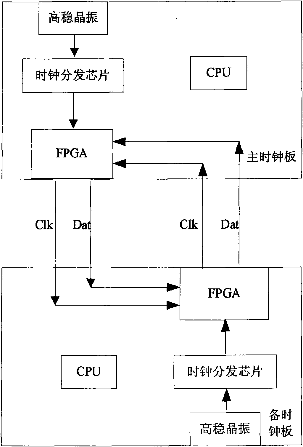
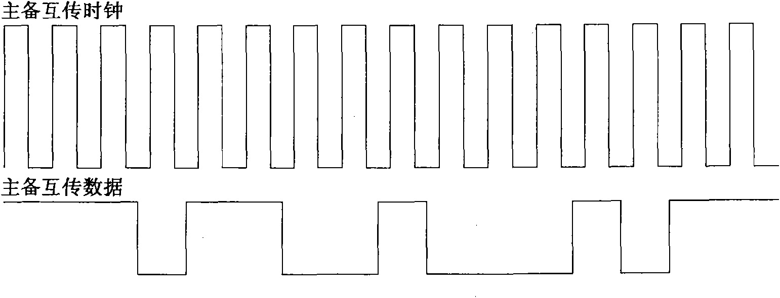
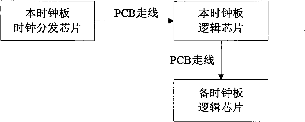
[0056] Such as figure 1 As shown, the system for realizing master-standby clock switching in this embodiment includes a master clock board and a slave clock board, both of which have a CPU, a clock source of the same frequency, a clock distribution chip and a logic chip. The logic chip of this embodiment is implemented by a Field Programmable Gate Array module (Field Programmable Gate Array, FPGA for short), and the same-frequency clock source is implemented by a high-stable crystal oscillator. The clocks of the main clock board and the standby clock board respectively track the same-frequency high-stable crystal oscillator of the clock board, so that the output frequencies of the main and standby clocks are basically the same. The logic chips of the main clock board and the standby clock board are connected by two pairs of mu...


PUM


Abstract

The invention discloses a method for switching main and backup clocks, which is applied to a system comprising a main clock board and a backup clock board. Clock generation chips of the main clock board and the backup clock board respectively track a common-frequency clock source of the respective clock board; the mutual transmission of the main and backup clocks and data is achieved through respective logic chips; when the main and backup clocks are to be switched, a pre-switching instruction is sent to the logic chip of the main clock board, and after receiving the instruction, the logic chip of the main clock board sends a synchronous instruction to the logic chip of the backup clock board; after receiving the synchronous instruction, the logic chip of the backup clock board sends an effective synchronous signal in a pulse form to the clock generation chip of the backup clock board; and the clock generation chip of the backup clock board stops the clock output when the synchronous signal is effective, and restores the clock output after first delay time when the synchronous signal is not effective, phase positions of the main and backup clocks are aligned, and the main and backup clocks are instructed to execute main and backup switching. The method cannot cause phase position transient variation, unstable system and poor reliability due to the switching, and simultaneouslyhas less occupied resources.

Description

technical field [0001] The present invention relates to the switchover of master and backup clocks, and more specifically, to a method and system for switching master and backup clocks. Background technique [0002] The clock is a key signal of the communication equipment, and the various performances of the clock will affect the performance of the single board and even the whole system. Therefore, it is very important for the communication equipment to ensure the accuracy and stability of various performances of the communication equipment clock. Therefore, all communication organizations, countries and operators must strictly test the performance of the clock of the device before the device is connected to the network. The performance indicators of the clock mainly include frequency and phase. Usually, the performance of the above indicators includes long-term stability, long-term accuracy, hold performance, phase transient and phase discontinuity, etc. [0003] Communic...

Claims


Application Information

Patent Timeline
Patent Type & Authority Applications(China)
IPC IPC(8): H04L7/00H04L1/22
Inventor 柳旺李宗安傅小明
Owner ZTE CORP
Why Eureka
Try Eureka