Pin wiring structure of card insertion end of flexible printed circuit board

A flexible printing and circuit board technology, applied in the directions of printed circuit components, secondary processing of printed circuits, reinforcement of conductive patterns, etc., can solve the problems of process accuracy and pin width limitations, breakage of traces 2110, short circuits, etc.

Inactive Publication Date: 2010-03-10
WINTEK CORP
View PDF0 Cites 5 Cited by
  • Summary
  • Abstract
  • Description
  • Claims
  • Application Information

AI Technical Summary

Problems solved by technology

The staggered pins 211 and 212 are formed by electroplating (the pin 211 is an odd-numbered pin, and the pin 212 is an even-numbered pin). In order to achieve a staggered configuration, the pin 211 will have part of the wiring 2110 and the

Method used


Image

  • Pin wiring structure of card insertion end of flexible printed circuit board
  • Pin wiring structure of card insertion end of flexible printed circuit board
  • Pin wiring structure of card insertion end of flexible printed circuit board

Examples


Embodiment Construction

[0051] See Figure 3A , Figure 3B and Figure 3C , which is a schematic diagram of the wiring structure of the pins at the card end of the flexible printed circuit board of the present invention, wherein Figure 3A and Figure 3B for the top view, Figure 3C is a sectional view.

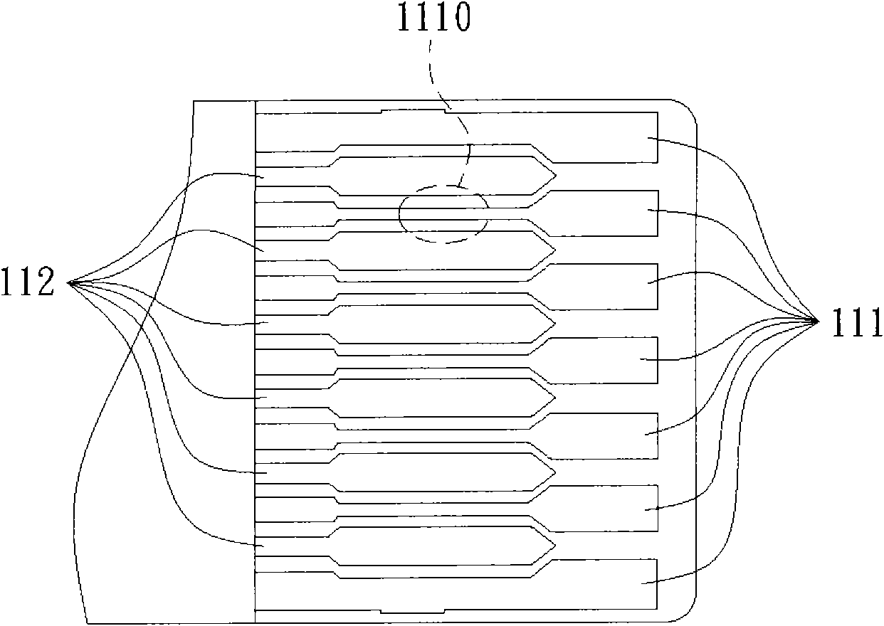
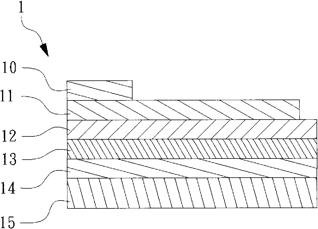
[0052] The card insertion end 3 of the flexible printed circuit board of the present invention is sequentially provided with a first protective layer 30, a first conductive layer 31, a substrate 32, a second conductive layer 33, and a second protective layer. 34 and a reinforcing plate 35 are stacked, and the first conductive layer 31 and the second conductive layer 34 can be made of metallic copper.

[0053] The first conductive layer 31 is formed with a plurality of first traces 311 (parts of the first traces 311 are covered by the first protection layer 30, indicated by dotted lines), and one end of each of the first traces 311 is respectively extended with a first A pin 312, the first cond...


PUM


Abstract

The invention discloses a pin wiring structure of a card insertion end of a flexible printed circuit board, which comprises a substrate, a first conductive layer, a second conductive layer and a plurality of conducted elements, wherein the first and second conductive layers are arranged on the two surfaces of the substrate respectively; the first conductive layer is provided with a plurality of first wires; the second conductive layer is provided with a plurality of second wires; the first wires electrically extend a plurality of first pins and are provided with a plurality of second pins in different positions from the first pins; the second wires are correspondingly extended to the corresponding positions of the second pins; and the conducted elements are electrically communicated to thesecond pins and the second wires respectively so that the second pins, the first wires and the first pins are in a non-contacted off state to form the card insertion end of the flexible printed circuit board with two layers of wires.

Description

technical field [0001] The present invention relates to a pin wiring structure of a flexible printed circuit board card-inserting end, in particular to a pin wiring structure of a flexible printed circuit board card-plugging end with a layered wiring structure. Background technique [0002] Generally, the pin routing structure of the flexible printed circuit board on the market is mainly made with reference to the recommended size in the connector specification book. The line width and line spacing of the staggered pins (pins) are small, and to avoid insertion into the connector (connector), its internal pins contact with the adjacent pins of the flexible printed circuit board to cause a short circuit, so the dimensional tolerance control of the staggered pins is also more precise. [0003] Nowadays, connectors with a large number of pins are used more and more frequently. The larger number of pins means that the size of the card insertion side must be larger, but the dimens...

Claims


Application Information

Patent Timeline
IPC IPC(8): H05K1/11H05K3/24
Inventor 罗启文王月芳
Owner WINTEK CORP
Why Eureka
Try Eureka