Production technology of PCB (Printed Circuit Board) solder mask

A printed circuit board and production process technology, which is applied to the secondary treatment of printed circuit, coating of non-metallic protective layer, etc., can solve the problems of film printing and developing side erosion, unclean development, red lines, etc., and achieve improvement The effect of production efficiency and production quality, reduction of production cost, and acceleration of production progress

Active Publication Date: 2010-03-10
大连崇达电子有限公司
View PDF0 Cites 51 Cited by
  • Summary
  • Abstract
  • Description
  • Claims
  • Application Information

AI Technical Summary

Problems solved by technology

[0004] In order to better overcome the disadvantages such as green oil and other solder resist oil plugging holes, dirty development, red lines, large film printing and developing side erosion, etc. in the production process of the above-mentioned printed circuit board solder mask layer, the present invention provides A production process of solder resist layer for printed circuit board

Method used


Image

  • Production technology of PCB (Printed Circuit Board) solder mask

Examples


Embodiment Construction

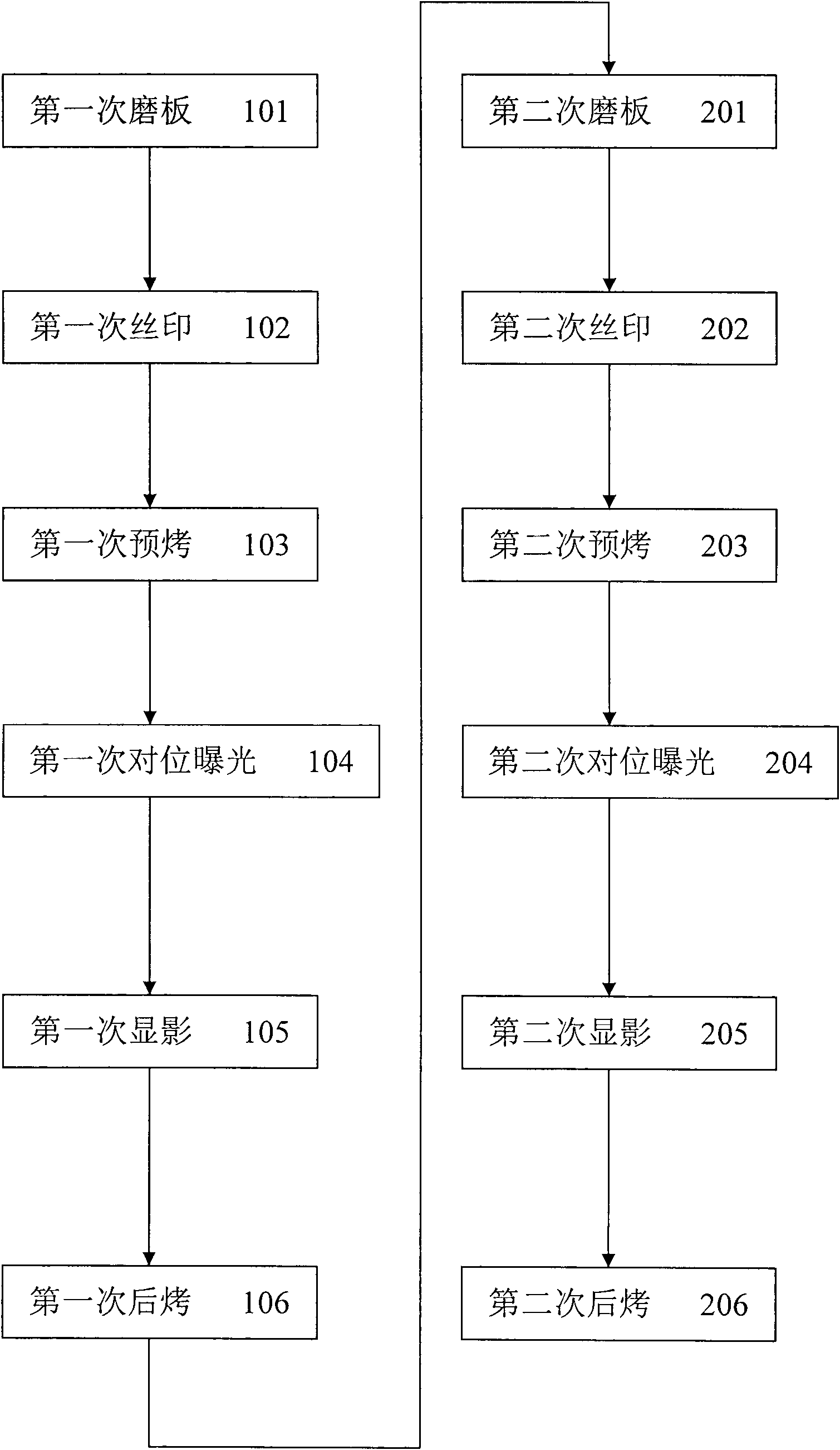
[0015] Below in conjunction with accompanying drawing and specific embodiment the present invention will be described in further detail: as figure 1 As shown, a production process of a printed circuit board solder resist layer includes the following steps: the first grinding plate 101, the first silk screen printing 102, the first pre-baking 103, the first alignment exposure 104, the first Developing 105, first post-baking 106, second grinding plate 201, second silk screen printing 202, second pre-baking 203, second alignment exposure 204, second developing 205, second post-baking 206, The mesh number of the first silk screen 102 is greater than the mesh number of the second silk screen 202, and the window size of the first alignment exposure 104 (that is, the size of the solder pad after processing) is larger than the first time. The window size of the secondary alignment exposure 204 .

[0016] By controlling the mesh number of the first silk screen 102 to be greater than t...


PUM


Abstract

The invention relates to a production technology of a PCB (Printed Circuit Board) solder mask, which comprises the following steps of: a first board grinding, a first silk screen, a first pre-braking,a first contraposition exposure, a first development, a first post-baking, a second board grinding, a second silk screen, a second pre-braking, a second contraposition exposure, a second developmentand a second post-baking, wherein the mesh number of the first silk screen is larger than that of the second silk screen, and the windowing size of the first contraposition exposure is larger than that of the second contraposition exposure. The production technology of the PCB solder mask better eliminates the harmful defects in the solder mask production process that green oil and the like easilysolders an oil plughole, the developing is dirty, the circuit becomes red, and the lateral erosion of a film printing and development is large and the like, thereby improving the production efficiency and the production quality, speeding up the production schedule and reducing the production cost.

Description

【Technical field】 [0001] The invention belongs to the field of printed circuits, in particular to a production process for a solder resist layer of a printed circuit board in the field of printed circuits. 【Background technique】 [0002] A printed circuit board (PCB) mainly includes pads, vias, solder mask, silk screen and other parts. The green or brown, red, yellow, etc. on the printed circuit board are generally the color of the solder resist paint. This layer is an insulating protective layer, called the solder resist layer. [0003] With the development of the electronics industry, the requirements for printed circuit boards are getting higher and higher. The high density, thin wires, and small apertures of printed circuit boards are becoming faster and faster, and the requirements for the production process of the solder mask layer of printed circuit boards are also getting higher and higher. higher and higher. At present, in the solder mask production process of pri...

Claims


Application Information

Patent Timeline
Patent Type & Authority Applications(China)
IPC IPC(8): H05K3/28
Inventor 刘克敢
Owner 大连崇达电子有限公司
Why Eureka
Try Eureka