Small-carrier flat-four-side pin-less packaging part and preparation method thereof

A leadless package and four-sided flat technology, which is applied in semiconductor/solid-state device manufacturing, electric solid-state devices, semiconductor devices, etc., can solve the problems of restricting product profit margins, long bonding wire length, and high bonding wire cost

Active Publication Date: 2010-04-21
TIANSHUI HUATIAN TECH
View PDF1 Cites 33 Cited by
  • Summary
  • Abstract
  • Description
  • Claims
  • Application Information

AI Technical Summary

Problems solved by technology

However, at present, the QFN (0707×0.75-0.50) carrier is large, and the length of the inner pin is fixed. When the IC chip is small, the length of the bonding wire is long, resulting in a high cost of the bonding wire, which restricts the profit margin of the product.

Method used


Image

  • Small-carrier flat-four-side pin-less packaging part and preparation method thereof
  • Small-carrier flat-four-side pin-less packaging part and preparation method thereof
  • Small-carrier flat-four-side pin-less packaging part and preparation method thereof

Examples


Embodiment 1

[0057] 1. Thinning and scribing

[0058] Thinning thickness is 50μm, stack package, roughness Ra 0.10mm.

[0059] 8″ wafer thickness reduction: DR3000III / NITI0 for placement machine,

[0060] 8″ thinning machine: PG300RM / TSN. Thickness gauge DH151 / TSK;

[0061] 8″ dicing machine: WD300TXB, DR3000III / TSK for SMT.

[0062] Anti-separation layer, anti-shards process scribing.

[0063] 2. Core loading

[0064] 8″ choose AD829 or AD889 core loading machine;

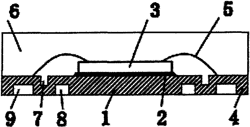
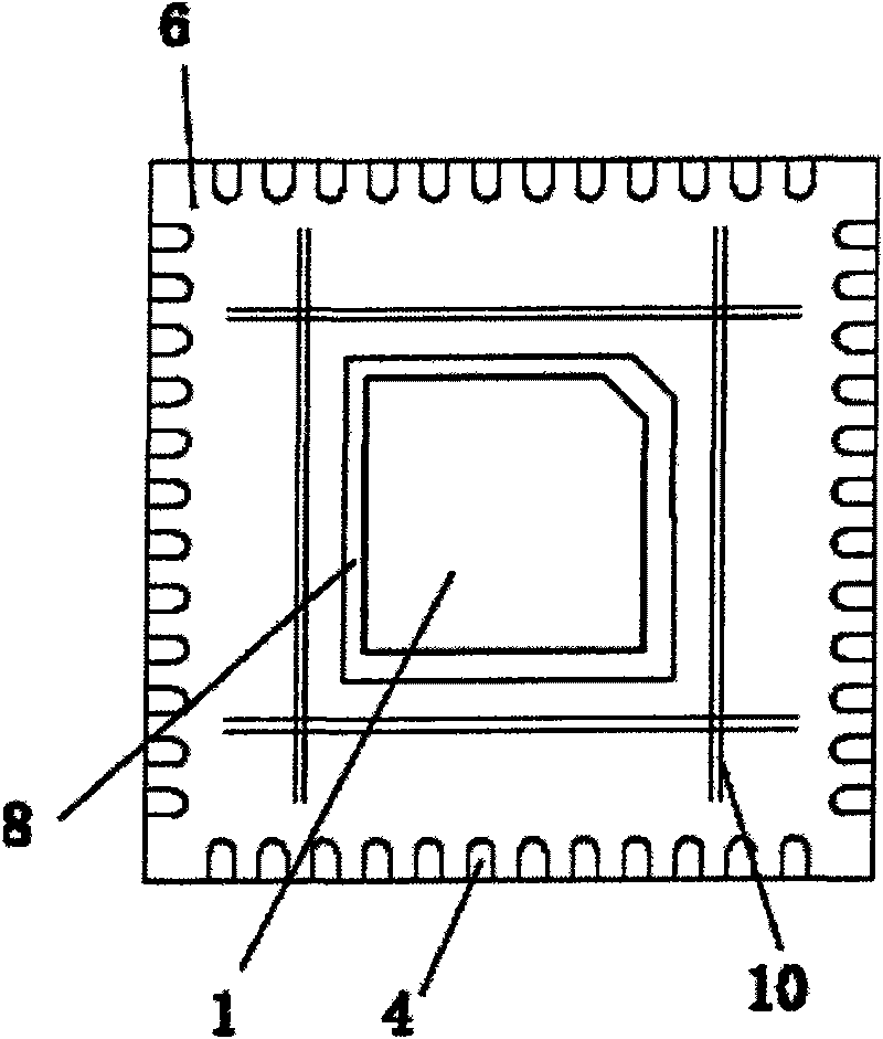
[0065] Adhesive film is used as the bonding material, and the lead frame is a four-sided flat leadless frame with double rows of pins, and the film baking process is used.

[0066] 3. Pressure welding

[0067] ESEC3100 and Eagle60 bonding machines are selected, and gold wire is used as the welding wire material. Since the thickness of the package is 0.75, the pressure welding adopts the ultra-low-line arc pressure welding process, and the high-low arc positive and negative bonding method avoids the phenomenon of cross-wi...

Embodiment 2

[0080] 1. Thinning and scribing

[0081] Thinning thickness 200μm stacked package, roughness Ra 0.05mm.

[0082] 12″wafer thickness reduction: DR3000III / NITIO for placement machine,

[0083] 12″ thinning machine: PG300RM / TSN. Thickness gauge DH151 / TSK;

[0084] 12″ dicing machine: WD300TXB, DR3000III / TSK for SMT,

[0085] Anti-separation layer, anti-shards process scribing.

[0086] 2. Core loading

[0087] 12″ choose DB-700FC / Jupei chip bonder.

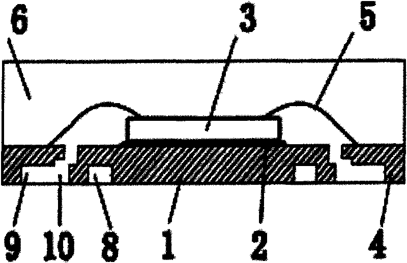
[0088] Adhesive film material: Insulating film is used, the lead frame is a four-sided flat leadless frame with double rows of pins, and the film baking process is used.

[0089] 3. Pressure welding

[0090] Eagle60 bonding machine is used for pressure welding, copper wire is used for welding wire material, ultra-low arc pressure welding process is adopted for pressure welding, and high and low arc positive and negative welding methods are used to avoid wire crossing and broken wires. The inner row of pins adopts low arc weldi...

Embodiment 3

[0104] 1. Thinning and scribing

[0105] According to the thickness of the packaged product, the thinning thickness is determined to be 100 μm, and the roughness is controlled at Ra 0.08mm.

[0106] 8″ wafer thickness reduction: DR3000III / NITI0 for placement machine,

[0107] 8″ thinning machine: PG300RM / TSN. Thickness gauge DH151 / TSK;

[0108] 8″ dicing machine: WD300TXB, DR3000III / TSK for SMT.

[0109] Anti-separation layer, anti-shards process scribing.

[0110] Other processes are the same as in Example 1.


PUM


Abstract

The invention relates to a small-carrier flat-four-side pin-less packaging part, which comprises a lead frame carrier, a bonding sheet adhesive, an IC chip, a soldering-pan on the IC chip, a bonding line and a plastic-packaged body. The packaging part is characterized in that: before cutting separation, all inner pins extend inwards to connect with the carrier; a groove is formed between the carrier and the inner pins; the bottom parts of the inner pins are provided with grooves, and the backside of the carrier is provided with a circle of anti-flash groove. The packaging part is processed and produced through the process steps of thinning, scribing, chip loading, press welding, plastic packaging, electroplating, cutting and the like. The small-carrier flat-four-side pin-less packaging part has the characteristics that the carrier is reduced, the inner pins extend inwards to connect with the carrier before the cutting separation, the connection part of the inner pins and the carrier is provided with a 0.10 mm pit, the pin length outside the pit is 1 mm longer than that of a common QFN pin, and the lower part of the carrier is provided with a circle of the anti-flash groove which can prevent flashes from continuously dispersing towards the backside of the carrier.

Description

technical field [0001] The invention relates to the technical field of electronic information automation component manufacturing, in particular to a small carrier four-sided flat leadless package, and the invention also includes a preparation method of the package. Background technique [0002] In recent years, the market for portable electronic devices in the field of mobile communications and mobile computers has exploded, directly promoting the development of small packaging and high-density assembly technologies. At the same time, a series of strict requirements are also put forward for small package technology, such as requiring the package size to be reduced as much as possible, especially the package height is less than 1mm; the reliability of the packaged product is improved as much as possible, in order to protect the environment and adapt to lead-free soldering, and Try to reduce costs. There are many miniaturized packaging structures, such as ball grid array BGA ...

Claims


Application Information

Patent Timeline
Patent Type & Authority Applications(China)
IPC IPC(8): H01L25/00H01L23/48H01L23/13H01L23/495H01L21/50
CPCH01L2224/73265H01L2224/32245H01L2224/48247H01L2224/45147H01L24/73H01L2224/45015H01L2224/45144H01L2224/48091H01L2924/14H01L2924/181H01L2924/00012H01L2924/207H01L2924/00014H01L2924/00
Inventor 郭小伟慕蔚
Owner TIANSHUI HUATIAN TECH
Why Eureka
Try Eureka