Fine-pitch single IC chip packaging part and preparation method therefor

A technology of chip packaging and details, which is applied in semiconductor/solid-state device manufacturing, electrical components, electric solid-state devices, etc. It can solve problems such as difficulty in controlling the diameter of bonding balls, damage to the previous wire, and short-circuiting of adjacent solder joints. Achieve the effect of avoiding short circuit of adjacent solder joints, reducing the punching rate of plastic packaging, and excellent bonding strength

Inactive Publication Date: 2017-12-19
长沙安牧泉智能科技有限公司
View PDF6 Cites 4 Cited by
  • Summary
  • Abstract
  • Description
  • Claims
  • Application Information

AI Technical Summary

Problems solved by technology

[0005] However, for the bonding of fine-pitch pads, the diameter of the bonding ball is difficult to control. If you are not careful, the bonding ball will exceed the pad, causing a short circuit between adjacent solder joints, resulting in product scrapping
In addition, because the distance between the lines is too small, when the second line is played, it will touch the previous line, causing damage to the previous line.

Method used


Image

  • Fine-pitch single IC chip packaging part and preparation method therefor
  • Fine-pitch single IC chip packaging part and preparation method therefor
  • Fine-pitch single IC chip packaging part and preparation method therefor

Examples


Embodiment

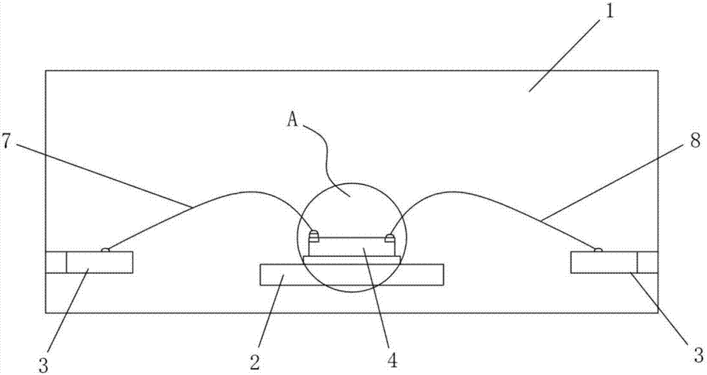
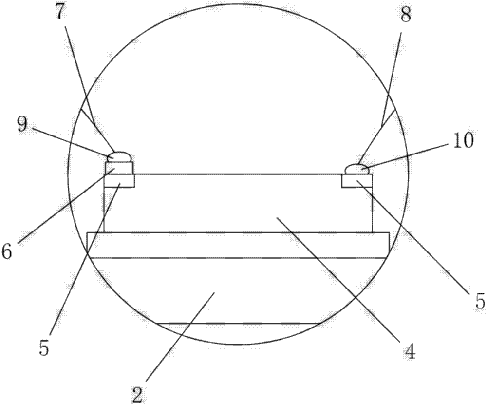
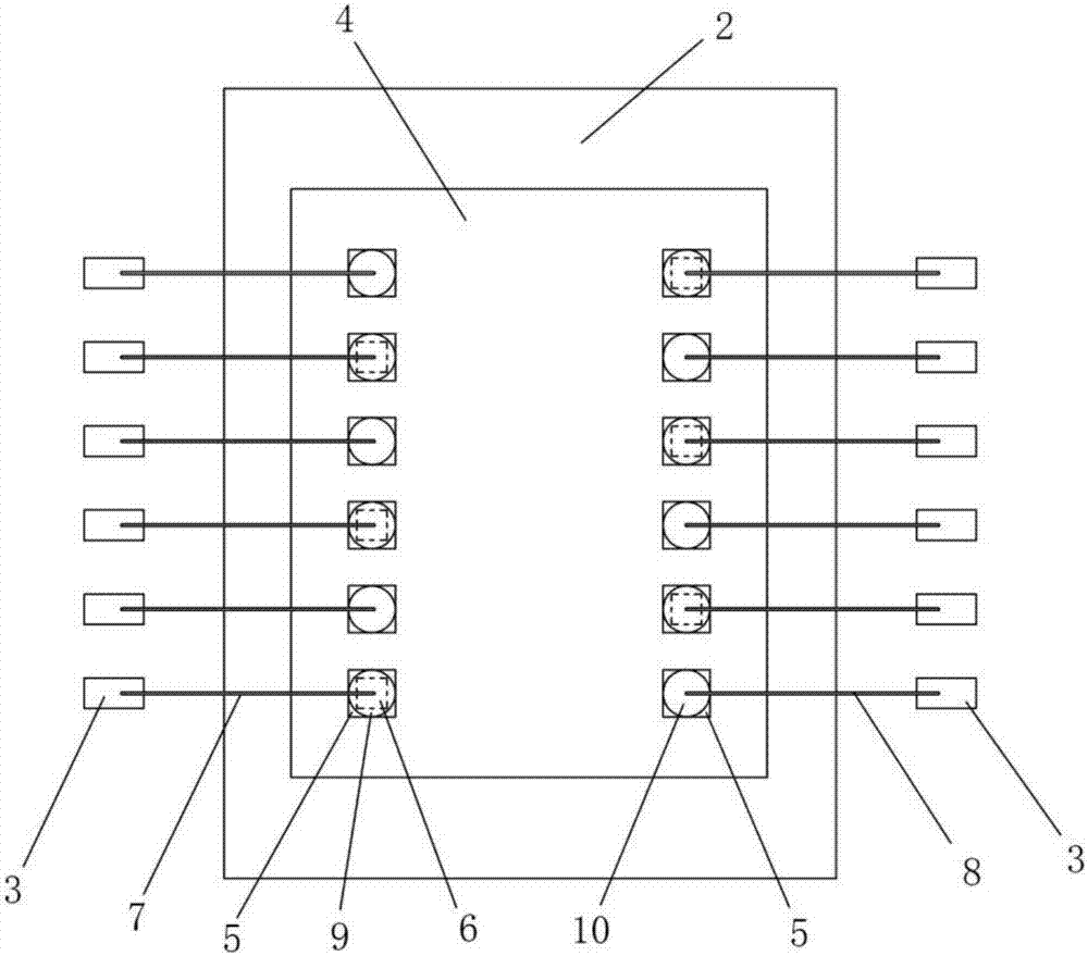
[0033] A kind of fine-pitch single IC chip package of the present invention, its structure is as Figure 1 to Figure 4 shown, by Figure 1 to Figure 4 It can be seen that it mainly includes a plastic package body 1, and a lead frame carrier 2 and a plurality of frame lead inner pins 3 are arranged in the plastic package body 1, and an IC chip 4 is fixed on the upper surface of the lead frame carrier 2 through an adhesive. A plurality of bonding pads 5 are provided on the upper surface of the chip 4 . The pads 5 are arranged in parallel in two rows to form a first pad group and a second pad group. Each pad 5 is respectively connected to a pin 3 in the frame lead through a copper bonding wire. Aluminum electroplating layers 6 are arranged at intervals on the upper surfaces of the plurality of pads 5 in each pad group. The pads 5 provided with the aluminum electroplating layer 6 in one pad group correspond to the positions of the pads 5 not provided with the aluminum electropl...


PUM


Abstract

The invention discloses a fine-pitch single IC chip packaging part and a preparation method therefor. The packaging part comprises a plastic packaging body; a lead framework carrier and multiple framework lead inner pins are arranged in the plastic packaging body; an IC chip is fixedly connected with the upper surface of the lead framework carrier; multiple bonding pads are arranged on the upper surface of the IC chip; the multiple bonding pads are arranged in parallel in two rows to form a first bonding pad group and a second bonding pad group; each bonding pad is connected with one corresponding framework lead inner pin through a copper bonding line; aluminum electroplating layers are arranged at intervals on the upper surfaces of the multiple bonding pads in each bonding pad group; and the bonding pads, provided with the aluminum electroplating layers, in one bonding pad group, are corresponding to the bonding pads, not provided with the aluminum electroplating layers, in the other bonding pad group. Adjacent welding points in the packaging part do not suffer from short circuit easily, so that high product yield and good quality are realized; and the preparation method is low in cost and high in production efficiency.

Description

technical field [0001] The invention relates to the technical field of electronic component manufacturing, in particular to a fine-pitch single IC chip package and a preparation method thereof. Background technique [0002] In contemporary times, the chip manufacturing industry has rapidly entered the nanometer era with the rapid development of the electronics industry. The process size of chip manufacturing has shrunk from the initial 90nm to the current 13nm or even lower. The geometric size of the chip is therefore reduced to the current 0.15mm × 0.15mm. Correspondingly, the pad pitch and scribe line used in chip manufacturing are also gradually reduced to 45 μm. The size of the pad is also gradually reduced to the current 38μm×38μm. This dimensional variation brings a series of difficulties and challenges to the bonding process. [0003] Usually, in the ball bonding process, the qualification standard of the solder ball is that the diameter is greater than or equal to...

Claims


Application Information

Patent Timeline
Patent Type & Authority Applications(China)
IPC IPC(8): H01L23/488H01L21/50H01L21/60
CPCH01L21/50H01L23/488H01L24/10H01L24/85H01L2224/10122H01L2224/85007H01L2224/85051H01L2924/01029H01L2224/05554H01L2224/48091H01L2224/48247H01L2224/49107H01L2224/49175H01L2224/73265H01L2924/181H01L2924/00014H01L2924/00012
Inventor 朱文辉杨辉李军辉何虎陈卓
Owner 长沙安牧泉智能科技有限公司
Why Eureka
Try Eureka